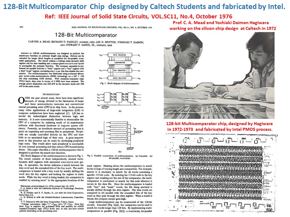
**********************
The AIPS ( Artificial Intelligent Partner System ) Home Page 010
hagiwara-yoshiaki@aiplab.com
Return to http://www.aiplab.com/
**********************
For full English versions, please visit the following sites.
Story of Pinned Photo Diode (html)
Hagiwara at SONY is the true inventor of Pinned Photo Diode (html)
See also ElectronicsStackExchangeSite on "What is Pinned Photo Diode ? "
Pinned Photo Diode was invented by Hagiwara of Sony in 1975 (PDF)
**********************
******************************
Yoshiaki Hagiwara, Ph.D. IEEE Life Fellow、
Pinned Photo Diode の発明者は もとSONYの萩原良昭です。
******************************
その証拠は萩原が1975年に出願した日本国特許 (1975-127647) と
(1975-134985)に詳細に記載されています。1978年にSONYは萩原が
発明したPinned Photo Diode を搭載した Frame Transfer方式の
CCD image sensor 搭載のビデオカメラの原理試作をSONYの盛田
昭夫会長が New York で、同時に SONYの岩間和夫社長が東京で
新聞発表しています。
萩原の発明特許(1975-134985)の実施例を示す例図1から例図5には
Interline Transfer方式の CCD image sensor に適用した場合を
詳細に説明しています。
SONYは全社総力をかけてこのPinned Photo Diode 搭載の Interline
Transfer方式の CCD image sensor のビデオカメラを世界で最初に
SONY original HAD sensor の商標と登録し、SONY BRANDとして
世界のビデオカメラ市場を制覇することになりました。
その強みは、萩原が発明した、超感度で低雑音で、かつ残像のない、
高品質画像を提供する、SONY original HAD sensor 、すなわち
一般に Pinned Photo Diodeと呼ばれるものが搭載されているからです。
また、萩原の出願の2つの特許の例図には、残像のない動作が、
萩原発明のこの光感知素子で、可能であることを明示しています。
詳細は、萩原考案の日本国特許(1975-127647) の実施例図7と、
萩原考案の日本国特許(1975-134985) の例図6に描かれています。
また、萩原考案の日本国特許(1975-127647) の短くて簡単な特許請求
範囲にはこの萩原考案の光感知素子は裏面照射型でも使用可能で
あることを明示しています。
また、その特許(1975-127647) には、埋め込み受光層が裏面からの
光照射を受けていることが描かれています。そして、表の面の電荷転送
用電極に信号電荷が完全電荷転送 Mode で転送されていることを、
その特許の実施例図7に明白に描かれています。
●以上の証拠より、Pinned Photo Diode の発明者は
もとSONYの萩原良昭であることは明白な事実です。
●この萩原提案は、すべての電荷転送装置(CTD)に適応されると
しています。つまり、BBD型でも、古典的なMOS型でもCCD型でも、
そして、近年脚光を浴びている CMOS 型の電荷転送装置(CTD)
にも、すなわち、CMOS image sensor にも適用できるとしています。
●さらに特許(1975-127647) の実施例図7の中では、裏面照射型の
CCD型 でも CMOS型でも適用可能な、Image Sensor 用光の
光感知素子構造 ( 一般に現在 Pinned Photo Diode と呼ばれる
構造)を世界で初めて提案しています。
●さらに特許(1975-134985) の実施例図4の中では、ショットキーバリア
型のImage Sensor 用光感知素子構造をも提案しています。
●しかし、次の様な受賞のニュースが入ってきました。
**************************************************************
2017 Queen Elizabeth Prize for Engineering Foundation.
**************************************************************
The winners of the 2017 Queen Elizabeth Prize
for Engineering Foundation were :
(1) George E. Smith for the CCD image sensor invention
(2) Michael Tompsett for the CCD image sensor development.
(3) Nobukazu Teranishi for the invention
of the pinned photodiode (PPD) and
(4) Eric Fossum for developing the CMOS image sensor.
**************************************************************
この受賞者の中で、もとNECの寺西さんが Pinned Photo Diodeの発明者
となっている事に、Pinned Photodiode (PPD)を発明した萩原は、また、
CMOS image sensor の開発者が Fossum となっている事に、いち早く、
CMOS image sensor の開発・商品化に成功したSONYの勤勉な技術者
チームは、あまりにもひどい事実誤認である事に驚いています。そこで、
第三者による公平な事実関係の確認をお願いしたい次第です。これは
半導体開発史およびその中でも重要な半導体素子のひとつでもある、
イメージセンサーの開発史にかかわる重要な事実関係の検証確認のお
願いです。はっきりと中立な公平な立場でコメントしていただける見識者の
方々を、萩原は現在個人的に探しております。半導体関連業界の学識者
の皆様におかれましてはぜひ萩原の主張する内容に関してご理解してい
ただき萩原をサポートしていただきたいと切に希望する次第でございます。
***************************************************************
**************************************************************************
Evidence that Hagiwara at Sony is the true inventor of the Pinned Photo Diode
**************************************************************************
Evidence that Hagiwara at Sony is the true inventor of the Pinned Photo Diode
is given by the two Japanese patents Hagiwara filed in 1975 at Sony. They are,
Japanese Patent (1975-127647) and (1975-134985). The evidence is described in
details in these two Hagiwara 1975 Japanese patents.
In 1978 Sony announced a new video camera in Tokyo and New York Press
Conferences at the same date, held by Sony Chairman Akio Morita in New York
and Sony President Kazuo Iwama in Tokyo at the same date in 1978.
The video camera was built with the Frame Transfer CCD image sensor
with the Hagiwara invented Pinned Photo Diode light detecting photo sensing
picture cell structure which has a very high light sensitivity, a very low noise
and a very low image lag features.
The figures N0.1 thru No.5 in Hagiwara Japanese patent (1975-134985)
explained in details an example of the interline transfer CCD image
sensor application with the Hagiwara invented Pinned Photo Diode.
Sony engineers, after the 1978 Press Conferences in Tokyo and New
York, worked hard for, and succeeded to acquire, the production
and the reliability technolgy of the CCD video camera of the interline
transfer CCD image sensor application with the Pinned Photo Diode
light detecting picture cell structure with the vertical overflow function.
With the diligent SONY engineers efforts, SONY could produce the
portable Passport size Compact CCD image sensor video camera, with
the Pinned Photo Diode that Hagiwara invented in 1975.
And at the same time, Sony filed a trading name officially, which
is the SONY Brand Name of " Sony original HAD sensor " .
With the help of the Hagiwara invented Pinned Photo Diode, which
was now called as " Sony original HAD sensor " with the strong
SONY original sales features of high light sensitivity, low noise and
no image lag characteristics, Sony could become soon very dominant
and strong over the world consumer video camera markets.
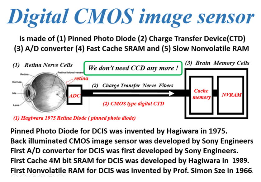
The feature of no image lag characteristics in the Hagiwara invented
Pinned Photo Diode is explained and shown in details, as an example
application case, in the figure No.6 of Hagiwara 1975 Japanese Patent
( 1975-134985 ) and also in the figure No.7 of Hagiwara 1975 Japanese
Patent ( 1975-127647 ) in details.
Hagiwara 1975 Japanese Patent ( 1975-127647 ) proposed a Back Light
illumiantion type light detecting photo sensing picture cell structure
with the buried layer type photo signal charge storage. And in the
figure No.7 of Hagiwara 1975 Japanese Patent ( 1975-127647 ) was
shown clearly how the signal charge in the buried storage layer are
trasfered completely to the region under the charge transfer gate
formed on the front side of the silicon wafer. This means clearly
the light sensing picture cell structure, which is now worldly called
as the Pinned Photo Diode, has the very important feature of no
image lag characteristics.
All of these Patent Claim descriptions and Patent figures for possible
patent application examples given in details in the two Hagiwara 1975
Japanese Patents ( 1975-127647 ) and ( 1975-134985 ) support the fact
that Hagiwara is the true inventor of the Pinned Photo Diode.
In conclusion, it is a clear cool fact that Hagiwara at Sony is the true
inventor of the Pinned Photo Diode. The Haiwara patents claims that
the light detecting picture cell structure ( now called as the Pinned
Photo Diode ) can be applied to any kind of charge transfer device(CTD)
which includes the BBD type, the classical MOS type, the CCD type and
the modern CMOS image sensor type charge transfer devices.
Hagiwara proposed the Pinned Photo Diode with the P+NPNsub junction
(thyrisor) type Light detecting picture cell structure with the vertical
over flow drain for the first time in the world.
Moreoever, Hagiwara proposed in the Japanese patent application example
of figure No.7 of Japanse patent (1975-126747) the Back Light illumination
Pinned Photo Diode type Light Detecting Picture Cell Structure for the
first time in the world.
Moreoever, Hagiwara proposed in the Japanese patent application example
of figure No.4 of Japanse patent (1975-134985) the Schottky Barrier type
Light Detecting Picture Cell structure in the Interline transfer type
CCD image sensor applicaiton for the first time in the world.
**************************************************************************
*******************************************************************
See three invited talks related to SONY HAD sensor now called also as Pinned Photo Diode.
(1) International Conference CCD79 in Edinburgh, Scotland UK
(2) International Conference ESSCIRC2001 in Vilach, Austria.
(3) International Conference ESSCIRC2008 in Edinburgh, Scotland UK
*******************************************************************
Hagiwara was invited in these international conferences because of his contributions
to the image sensor community and related digital system LSI chip design works.
*******************************************************************
However last year Hagiwara learned a very surprising news:
**************************************************************
2017 Queen Elizabeth Prize for Engineering Foundation.
**************************************************************
The winners of the 2017 Queen Elizabeth Prize for Engineering Foundation were :
(1) George E. Smith for the CCD image sensor invention
(2) Michael Tompsett for the CCD image sensor development.
(3) Nobukazu Teranishi for the invention of the pinned photodiode (PPD) and
(4) Eric Fossum for developing the CMOS image sensor.
**************************************************************
Hagiwara, the true inventor of the Pinned Photo Diode, got really
surprized at the announcement that Teranishi was awarded for the
invention of the pinned photodiode(PPD), and many SONY dilligent
engineers working for the compact digital CMOS image sensors
got really surprized at the announcement that Fossum was awarded
for developing the CMOS image sensor. The truth is that Teranish
did not invent the PPD. Teranish only developped in 1982 the image
lag free interline CCD image sensor with the PPD light detecting
photo sensor structure that was invented by Hagiwara in 1975.
Hagiwara 1975 patents clearly defined the image lag free interline
transfer CCD image sensor as an application example of his 1975
patent claims.
Fossum wrote a paper on "Active Pixel Sensors: Are CCD's
dinosaurs ?" , in Proc. SPIE, Vol.1900, pp.2-14, 1993. However,
the three transistor type active circuit was already invented by
Bill Regitz of Honeywell in 1969. This active pixel sensors was
not Fossum invention. Fossum actually did not develop the
active pixel sensors either. Sony dilligent engineerings did.
Fossum is not the inventor of the active image sensor picture element at all.
Peter Noble is the true inventor of the active image sensor picture element.
http://www.pjwn.co.uk/
Hitachi MOS Image Sensor Engineers and Intel MOS Process
Engineers all knew that eventually scaled down MOS Process
Technology will conquer all other kinds of Process Technologies
including CCD image sensor technology because of the power
consideration and scaled down dimensional advantage of CMOS
process technology. The three transistor CMOS active picture
cell was already invented as, since the three-transistor circuit
is identical to, the three-transitor circuit of the DRAM cell with
the active source follower type current amplification. Fossum
was just a commentator in his SPIE 1993 paper above. Fossum
was just emphasizing the well understood fact and speculations
that the original image sensor experts all knew in 1970s. This
active pixel sensors was not Fossum invention.Fossum actually
did not develop the active pixel sensors either.
Sony dilligent engineerings developped the active pixel Pinned
Photo Diode type Light detecting photo sensors for compact
digital CMOS image sensors with the Back Light Illumination.
**************************************************************
*******************************************************************
Questions by Prof. Albert Theuwissen are ,
- who invented and developed the stitching technology
for large area image sensors ?
- who owns the world record in low-noise
in the voltage domain for CMOS Image Sensor (CIS) ?
Hagiwara believes that
Hagiwara invented and Sony diligent engineers developed the stitching technology
for large area image sensors. SONY called SONY original HAD sensor.
But the technical world ignored the SONY businesss Brand Name HAD, and
called it by another name, the Pinned Photo Diode.
Sony diligent engineers developed and now Sony owns the world record in low-noise
in the voltage domain for CMOS Image Sensor (CIS).
******************************
to next Page011