**********************
The AIPS ( Artificial Intelligent Partner System ) Home Page 009
hagiwara-yoshiaki@aiplab.com
Return to http://www.aiplab.com/
**********************
For full English versions, please visit the following sites.
Story of Pinned Photo Diode (html)
Hagiwara at SONY is the true inventor of Pinned Photo Diode (html)
See also ElectronicsStackExchangeSite on "What is Pinned Photo Diode ? "
Pinned Photo Diode was invented by Hagiwara of Sony in 1975 (PDF)
**********************
Digital Camera by definition must be small and handy as originally conceived
by SONY with many semiconductor components, including the image sensor,
ADC, Fast Cache SRAM, the slow Nonvolatile memory chip and other digital
image processing units. One single engineer cannot develop all of it alone.
Many SONY deligent enginneers worked hard and developed the modern
CCD and CMOS digital Camera, with the P+NPNsub junction (thyristor)
type Light Dectecting Photo Diode ( JAP 1975-134985 ) and the N+NPN
junction type Buried Photo Diode ( JAP 1975-127647 ) with the back
light illumination scheme, both invented in 1975 by Hagiwara of Sony.
One person can invent it, but the many years of the hard working efforts
of many deligent people are needed to realize it.
*******************************************************************
萩原の母校のCaltech での在学時代、萩原は教授から
The truth shall you make you free.
という言葉を良く授業で聴かされました。その意味が、
萩原は、この歳、70歳になり、しみじみと感じています。
*******************************************************************
*******************************************************************
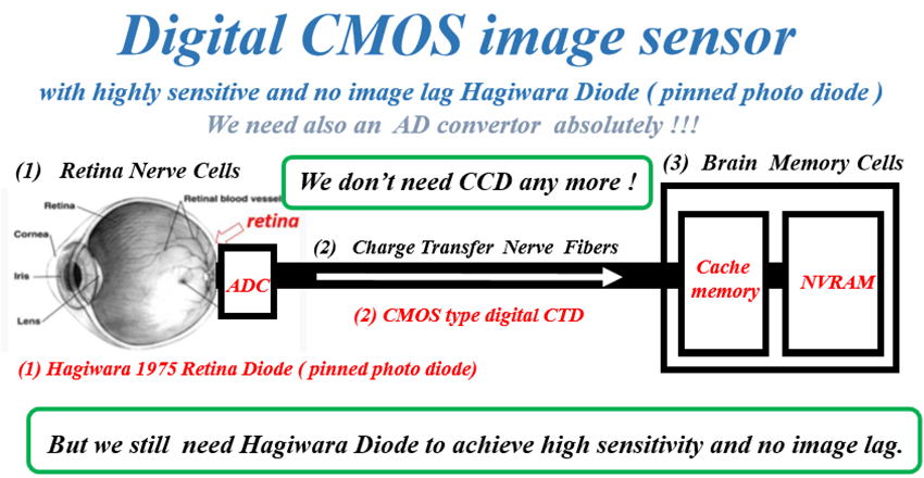
In 1960s, before CCD was invented, we already had beautiful color pictures
by the classical MOS image sensor with an excellent light sensitivity obtained
by the classical N+P junction type photo diode.
But to overcome the very large wire (CkT) noise, the three transistor
active source follower type circuits, invented by Peter Noble, was needed.
But the picture cell area was too small to incorporate this active circuit
in each picture cell area. We all knew that we had to wait untill we have
the complete MOS transistor process scale down, much furthur down.
(2) However, the CCD invention gave the image lag free and very low
wire (CkT) noise pictures. The CCD became the super star with the
help of the P+NPNsub junctiion (thyrsitor) type photo diode, which
was invented by Hagiwara in 1975. See JAP ( 1975-134985 ) .
CCD consumed a lot of power with only the transfer efficency of 99.999 %,
which was however possible to be applied for the classical NTSC picture
resolution. CCD had the serious trap noise and surface dark current problems.
Moreover, CCD had inherently MOS metal-type electrodes that do not pass
light and CCD was not as light-sensitive as the N+P photo diode. So, the CCD
type light detecting picture cell was replaced by the the P+NPNsub junctiion
(thyrsitor) type photo diode, Hagiwara 1975 invention. See JAP ( 1975-134985 ) .
In 1978, SONY annouced in New York and Tokyo Press Conferences the world
first CCD image sensor with no image lag, very highly light sensitive, low trap
noise, low surface dark current features of the PNP junction type photo diode
sensor pixel structure,Hagiwara 1975 invention. See JAP ( 1975-134985 ) .
At that time, the world already gave up the CCD image development efforts.
SONY was the only company that never gave up. Sony showed the future of
CCD image sesnor applications. The truth is that Hagiwara in SONY was the
only engineer in the world who did not give up. And Hagiwara showed the
future of CCD image sesnor applications. by the P+NPNsub junctiion type
photo diode, Hagiwara 1975 invention. See JAP ( 1975-134985 ) .
So Hagiwara save the CCD by his 1975 invention, which is now called by
another name, the Pinned Photo Diode.
The truth is that CCD was NOT highly light sensitive, NOT low dark current
and NOT trap noise free image sensor structure. The true super star was
not CCD. The true super star was hiden behind the curtain. The true super
star was Hagiwara 1975 invention, which is now called by another name,
the Pinned Photo Diode. SONY called it as the SONY original HAD sensor.
The truth is that the Pinned Photo Diode and the SONY original HAD sensor
are the same thing, that Hagiwara of SONY invented in 1975.
In conclusion, Hagiwara of SONY invented and his team of many dilligent
and hard working SONY engineers developed the stitching technology
for large area image sensors. The world followed after SONY efforts.
(3) Now, the complete CMOS transistor process scale down was achieved.
And the scale-downed three transistor active source follower type circuits,
originally invented by Peter Noble, can be now easily incorporated in each
picture cell of the CMOS image sesnors, with the help of the P+NP junctiion
type photo diode with the back light illumination scheme, which is again the
invention by Hagiwara in 1975. See JAP( 1975-127647 ).
SONY diligent and hard working engineers developed the modern dgital
CMOS image sensor with the back light illumination scheme for the
first time in the world.
Now again SONY owns the world record in low-noise in the voltage domain
for the modern digital CMOS image sensors (CISs).
Hagiwara 1975 invention ( JAP 1975-134985 ) helped CCD image sensor in the past.
Hagiwara 1975 invention ( JAP 1975-127647 ) is helping CMOS image sensor now.
Hagiwara and his original team of SONY diligent and hard working engineers developed
the stitching technology of both CCD and CMOS large area image sensors.
CCD was considered as the Super Star in the image sensor world in the past,
and the inventors were awarded with the NOBEL prize. But now CCD has
completely dissappeared from the modern digital image sensor world.
So who were the real super stars in the world ?
And now who are the real super stars in the world ?
*******************************************************************
*******************************************************************
Questions by Prof. Albert Theuwissen are ,
- who invented and developed the stitching technology
for large area image sensors ?
- who owns the world record in low-noise
in the voltage domain for CMOS Image Sensor (CIS) ?
*******************************************************************
Hagiwara believes that
Hagiwara invented it , in the Japanese 1975 patent ( 1975-134985 ) as the P+NPNsub
junction ( Thyristor ) type Light Detecting Picture Cell Structure, and Sony diligent
engineers, including Haggiwara, developed, the stitching technology for large area image
sensors. SONY called it as the SONY original HAD sensor technology in SONY business.
Naturally, the technical world did not use the SONY businesss Brand Name HAD, and
called it by another name, the Pinned Photo Diode. But the Pinned Photo Diode and
SONY original HAD are the same thing, both invented by Hagiwara in 1975.
At least, Teranishi did not invent the Pinned Photo Diode.
Hagiwara is the inventor of the Pinned Photo Diode.
Sony diligent engineers developed and now Sony owns
the world record in low-noise in the voltage domain for CMOS Image Sensor (CIS)
with the Pinned Photo Diode with the Back Light Illumination, that was also invented
by Haiwara of SONY in 1975 the Japanses 1975 patent ( 1975-127647 ).
At least, Fossum is not the inventor of the active image sensor picture element.
Peter Noble is the inventor of the active image sensor picture element.
http://www.pjwn.co.uk/
In the Fossum 2014 fake paper, Fossum attacked Hagiwara 1975 patent with lies,
insulting Sony and Hagiwara honor and pride on purpose. I could not understand
Fossum motivation. But I am now convinced that Fossum wanted Fossum himself
to be recognized by the world, with false explanations on Fossum friend Teranishi
as the TRUE inventor of the Pinned Photo Diode,NOT Hagiwara.
Fossum wanted to convince the world that Fossum himself developed the modern
CMOS digital camera. But now I understand that Peter and SONY diligent engineers
including Hagiwara. This is not fair at all. It is all lies. The world should know the truth.
Until last June I did not know what is the Pinned Photo Diode. I knew SONY HAD.
But I did not know myself that SONY HAD and the Pinned Photo Diode are the
same thing. My friends in Sony informed me that Teranish received awards from
Queen Elizabeth and Japanese Emperor as the inventor of the Pinned Photo Diode.
SONY diligent engineers were not happy at all. Maybe, Albert and Peter also felt it
as a bad news ? So I began to study what is Pinned Photo Diode last June.
Then I found the Fossum 2014 fake paper. I became really MAD at Fossum.
Besides, SONY won the SONY-NEC Patent war by Hagiwara 1975 patent
against the Teranishi1979 patent a long time ago. So Teranish should know that
Hagiwara is the inventor even though Teranishi published his work in IEDM1982.
Teranishi work was just a copy of Hagiwara 1975 patents that defined as one
Example case of Interline CCD image sensor with the complete charge transfer
Mode ( no image lag ) P+NPNsub junction type photon detector structure,
which is now called as the Pinned Photo diode.
But it is now more than four years after Fossum 2014 fake paper publication.
I found this fake paper, really too late.
I was very, very late since I do not belong to the image sensor community any more.
Yes, with my interests in the intelligent image sensors included, but my current major
interests are in the AIP ( Artificial Intelligent Partner ) systems, including AI software
and AI digital circuit system applications.
Yes, I try to be calm, but cannot be silent.
I feel that the world should know at least what is the truth.
I don’t think I can change the past history.
But people can learn the truth anytime, now and in future.
Yes, many people contributed.
Their deligence and efforts must be much worth recognitions.
*******************************************************************
http://www.aiplab.com/Hagiwara_at_Sony_is_the_true_inventor_of_Pinned_Photo_Diode.html
http://www.aiplab.com/Story_of_Pinned_Photo_Diode.html
http://www.aiplab.com/
*******************************************************************
*******************************************************************
以下にその根拠を説明するために萩原の1975年の2つの特許の説明をします。
[1] 特許 1975-127647 に関してですが、
1) 基体の片方の表の面に電荷転送部が設けられ
2) 基体の片方の表の面に沿って 第1の層(N)があり、
3)その第1の層(N)の中に、基体のもう片方の裏の面に沿って
受光電荷蓄積部(P)が埋め込まれ、
4) その受光電荷蓄積部(P)は上記の電荷転送部に隣接し、
5) 電荷転送部の電荷転送電極の印加する電圧により、
受光電荷蓄積部(P)の光信号電荷は電荷転送部に移動される。
すなわち、光感知素子は単純に NPN構造としています。
実施例図では、裏面から見て N+NPN 構造の Pinned Photo Diode です。かつ、その実施例から
その電荷転送が 埋め込み受光層(P)からの表の表面にある電荷転送部への完全空乏化電荷転送であり、
その結果、残像なしの特徴を示すことは明らかです。
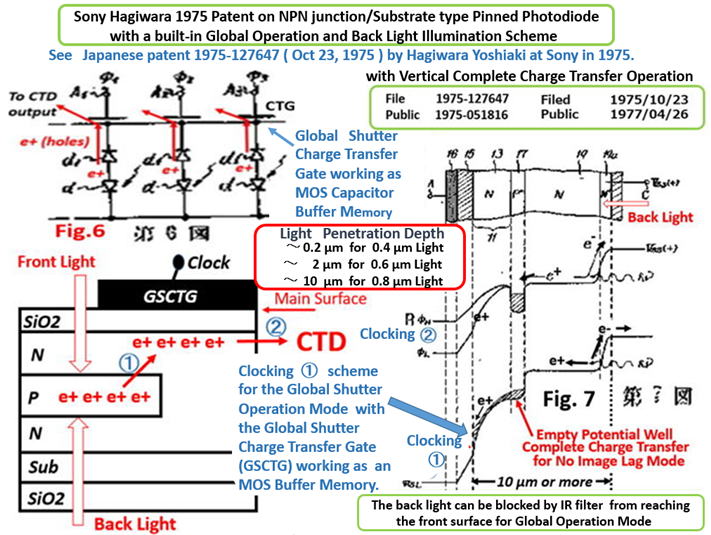
その 実施図には、裏面照射型の Pinned Photo Diode の例を
提示しています。完全空乏化電荷転送の様子も図示しています。
実際に裏面照射型を開発したのは、鈴木さんをはじめ、SONYの
技術者のみなさんです。
特許庁の文献(添付資料)には鈴木さんがその発明者となっていますが、
しかし、その基本構造はこの萩原の1975年の特許の例図に提示されています。
従って、萩原が最初の発明者(考案者)となるはずですが、
そう萩原は考えますが、いかがでしょうか?
ただし、萩原は発明しただけで、手をよごして開発したわけではありません。
SONYの技術者が総力をかけて開発し商品化したものです。
この特許の実施例として、裏面照射型のN+NPN 型の Pinned Photo Diode を
図示しています。従って、萩原がPinned Photo Diodeの発明者でもあります。
萩原の特許の実施図には完全空乏化電荷転送を明示しています。萩原発明の
この光感知素子構造( Pinned Photo Diode ) が完全残像なしの機能を有する
ことを意味しています。実施例には CCD IT 方式にも適用できると
明示しています。
NECの寺西さんは発明者ではありません。NECの寺西さんのチームは
萩原発明の構造(1977年に公開特許)を 1982年になり、原理試作し、
IEDM1982の国際学会で発表しました。「残像なしの IT CCD imager」として
発表したのは事実です。
世界初の、残像なしのIT方式のCCD image sensor は、SONYが開発し、
商品化しました。 1980年にSONYは、透明電極を採用して、横型OFDの
Two Chip IT CCD (萩原設計のもの)を商品化しています。残像のない
IT CCD imager をすでに商品化し、SONYは全日空のジャン機の
コックピットに搭載し、SONYの商品化したImage sensor の第1号でした。
こういう事実が、世間は詳細に正確にはその事実を知りません。
萩原の特許には、この萩原考案の Pinned Photo Diode が
IT方式のCCDにも適用できると明示されています。
このことを、しっかりSONYの名誉のためにも、萩原個人の名誉のためにも、
SONYの名誉を守るために、SONYの社員がまずしっかり理解していただき、
その利益代表者であるSONYとして、会社として、SONYのTOPが、公式に
発明協会の方々にSONYを主張であると同時に萩原の主張を、ご理解して
いただけるように、SONYのTOPが努力していただきたいです。
NECの寺西さんが発明者となると、SONYのHADも寺西さんの
発明という結論になります。これは矛盾します。SONYには
たいへん不名誉なことになります。
この萩原の主張を、SONYのみなさんにも、発明協会の関係者の
みなさんにもご理解していただきたいです。
[2] 特許 1975-134985に関してですが、その構造体の定義には、
特許請求範囲で定義された構造は
1) Nsubの基体に
2) 第1の導電層(P)があり、
3) その上に受光部で電荷蓄積部(N)があり、
4) この電荷蓄積部に接合(P+N)が形成される、
とあります。すなわち、P+NPNsub接合、すなわち、
サイリスタ―型の Pinned Photo Diodeを定義したものです。
特許請求文はいろいろな応用ケースが想定できるので、光感知部の
核となる構造のみを明確に定義しているだけの単純な構造特許です。
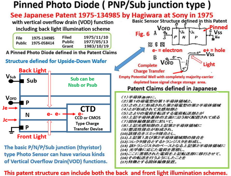
特許請求範囲は請求範囲を広いものにするため、文章での構造定義
としています。実施例はあくまで応用例で、特許請求範囲を束縛する
ものではありません。
特許請求範囲に定義された構造から専門家ならその具体的な構造を
イメージして、かつその構造の意味する動作は、半導体デバイスの構造
と動作を記述した教科書などの周知技術情報として、類推できます。
サイリスタ―のPunch-thru動作は教科書にあり周知の情報です。
さらに、Fairchild社所有のEarly 特許の光感知部はPhoto Diode でなく、
CCD構造のMOS型の受光構造です。SONYはそう主張に反論しました。
Fairchild社との縦型のOFDの特許戦争ではこの論理で Early 特許に
対してこの萩原特許を武器にしてSONYのImage Sensor ビジネスを守りました。
特許請求額は当時の金額で600億円以上とたいへん深刻な特許戦争でした。
NECからの特許攻撃の寺西特許(Buried Photo Diode特許 1980年)
に対しても萩原1975年の先行特許が、SONYのビジネスを守りました。
添付の資料では 縦型OFDは東芝の山田さんの発明となっています。
これも1975年の萩原発明のP+NPNsub接合(サイリスタ―)型の
構造は、縦型OFD機能を持った構造体であることは1977年には
萩原特許が公開された時点で世間一般の周知事実です。
東芝の山田さんの発明ではないことになると思うのですが、いかがでしょうか?
萩原の1975年の発明、すなわち、正確にはSONYの発明のはずです。
SONYの名誉、萩原の名誉のためにも、発明協会の方々に是非、
この事実関係をご確認いただき、ご理解いただくことは可能でしょうか?
この萩原の主張を発明協会の関係者のみなさんにもご理解していただきたいです。
こういう事実が、世間は詳細に正確にはその事実を知りません。
このことを、しっかりSONYの名誉のためにも、萩原個人の名誉のためにも、
SONYの名誉を守るために、SONYの社員がまずしっかり理解していただき、
その利益代表者であるSONYとして、会社として、SONYのTOPが、公式に
発明協会の方々にSONYを主張であると同時に萩原の主張を、ご理解して
いただけるように、SONYのTOPが努力していただきたいです。
この萩原の主張を、SONYのみなさんにも、発明協会の関係者の
みなさんにもご理解していただきたいです。
to next Page010