**********************
The AIPS ( Artificial Intelligent Partner System ) Home Page 004
hagiwara-yoshiaki@aiplab.com
Return to http://www.aiplab.com/
**********************
For full English versions, please visit the following sites.
Story of Pinned Photo Diode (html)
Hagiwara at SONY is the true inventor of Pinned Photo Diode (html)
See also ElectronicsStackExchangeSite on "What is Pinned Photo Diode ? "
Pinned Photo Diode was invented by Hagiwara of Sony in 1975 (PDF)
**********************
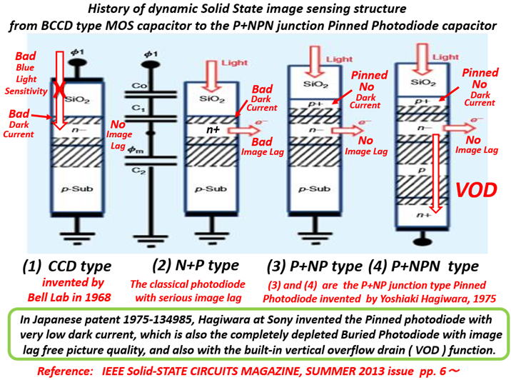
In the Hagiwara 1975 patent claims, it was clearly stated that the proposed light
detecting sensor cell structure, later called as Pinned Photo Diode which is
identical to the SONY original Hole Accumulation Diode (HAD), can be applied
to all kinds of the charge transfer device (CTD), which includes the classical
MOS type image sensor, the FT and ILT type CCD image sensors and also the
modern CMOS active pixel image sensor.
In the Hagiwara 1975 patent, application examples were given only for the
ILT type CCD image sensor. But the scope of the patent claims are not
limited by the application examples given in the patent figures.
The ILT type CCD application example was given because the ILT type CCD
image sensors were most promising at that time.
But as stated in the Hagiwara 1975 patent claims, the scope of the patents
includes all kinds of CTD including ITL type CCD and CMOS type image sensors.
The scope of the Hagiwara 1975 patent claims include, and hence can be applied
to, all kinds of the charge transfer device (CTD), including the classical MOS
type image sensor, the FT type and ILT type CCD image sensors and also the
modern CMOS active pixel image sensor.
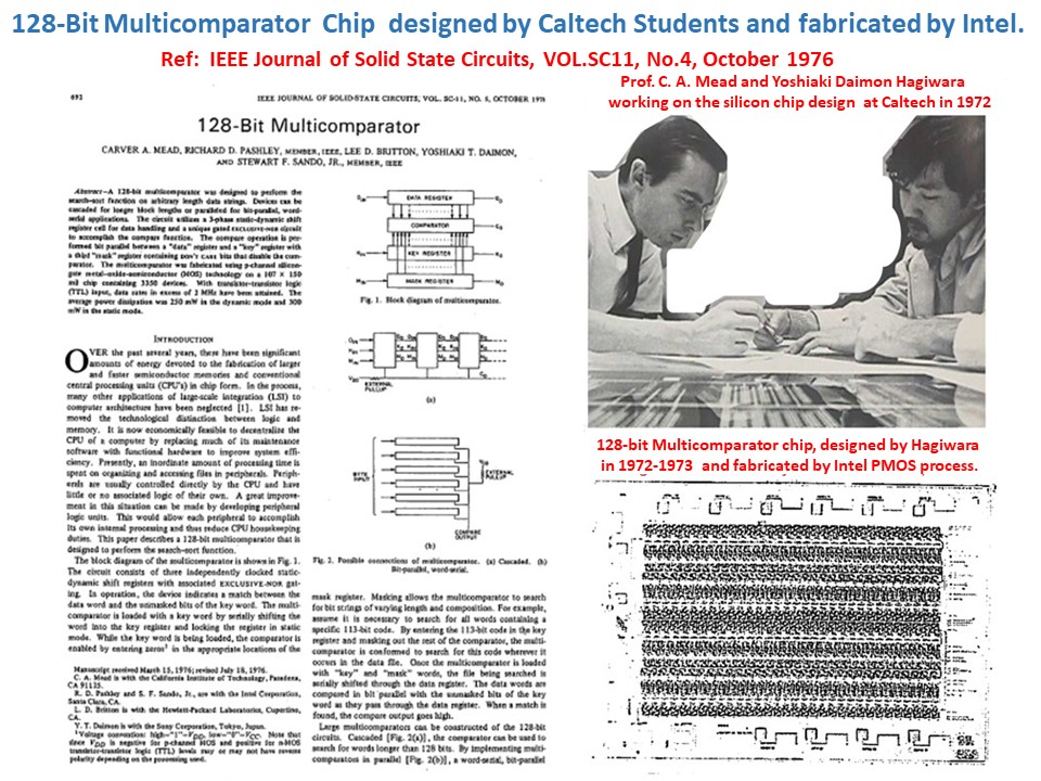
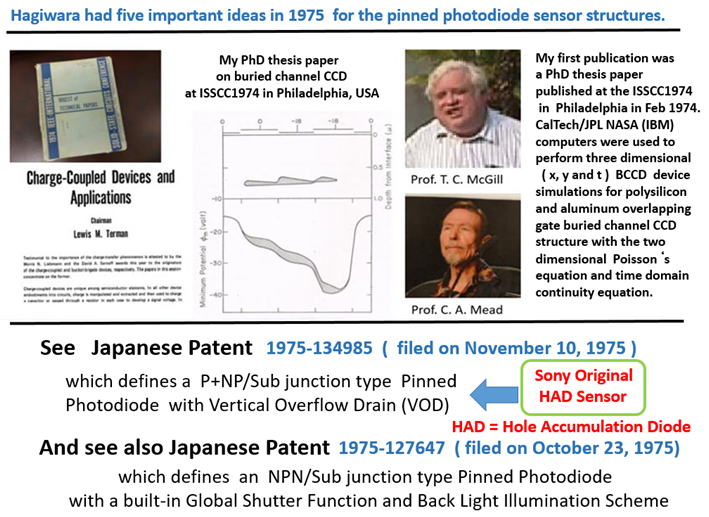
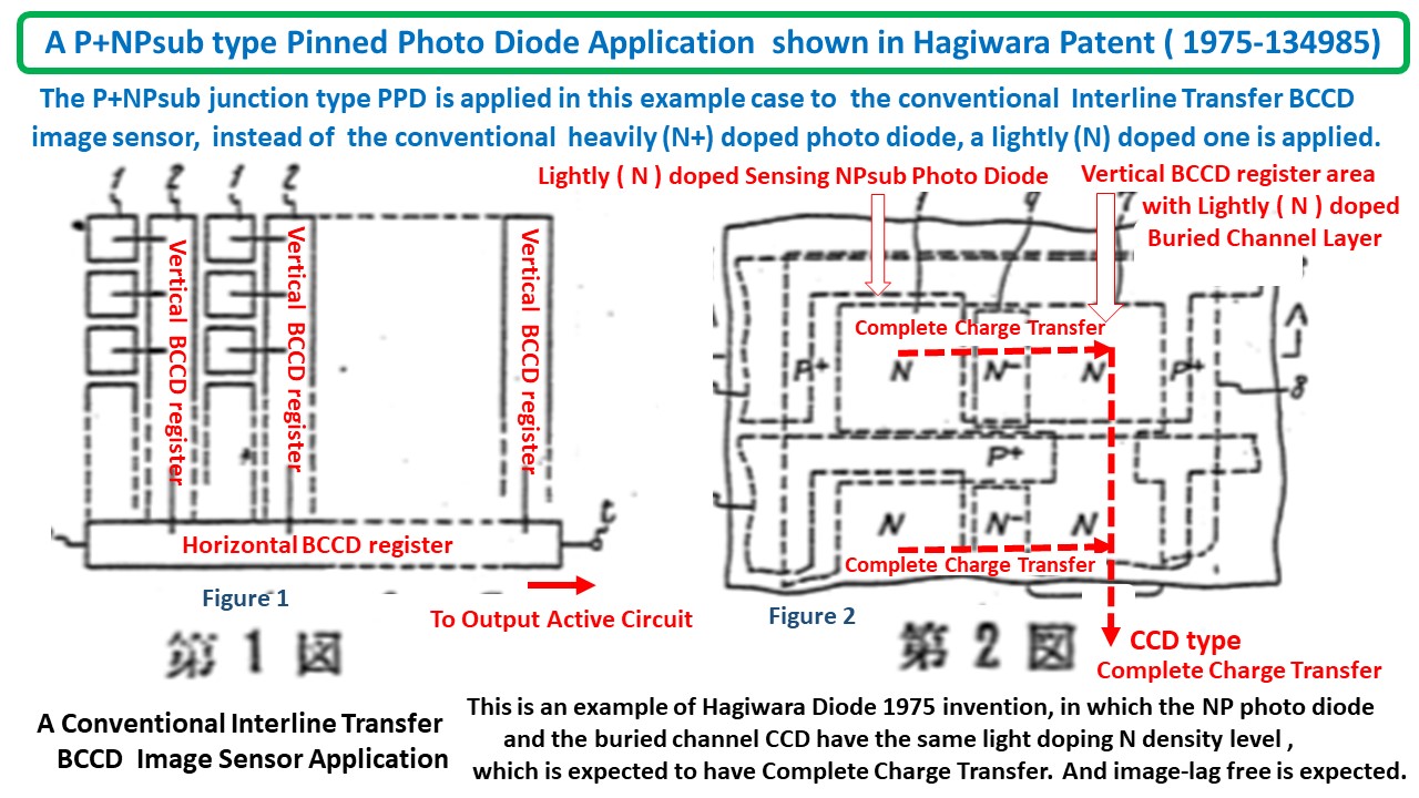
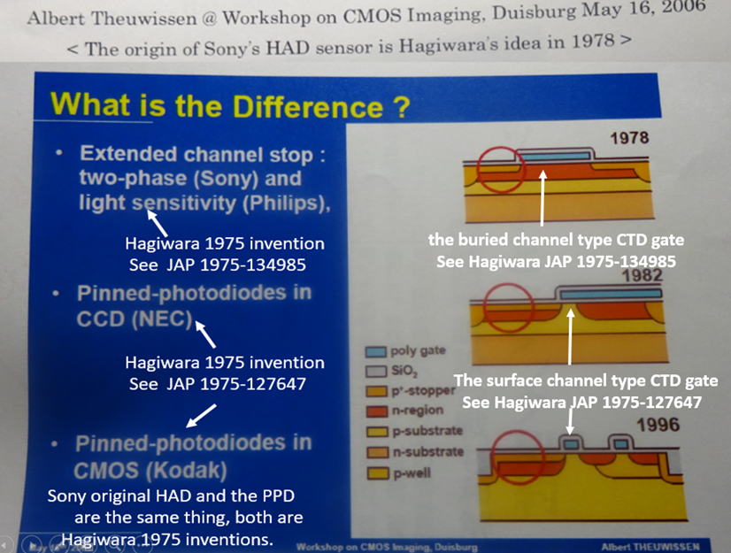
Hagiwara filed two patent. One is JAP 1975-127647 with the N+NPN type Pinned
Photo Diode, with the surface channel type CTD gate as an application example.
And the other is JAP 1975-134985 with the P+NPNsub junction ( thyristor ) type
Pinned Photo Diode, with the buried channel type CTD gate as an application example.
In these two patents, Hagiwara proposed both the Front Lihgt and the Back Light
illumination type Pinned Photo Diodes in 1975.
In the Hagiwara 1975 patent claims, it was clearly stated that the proposed light
detecting sensor cell structure, later called as Pinned Photo Diode which is
identical to the SONY original Hole Accumulation Diode (HAD), can be applied
to all kinds of the charge transfer device (CTD), which includes the classical
MOS type image sensor, the FT and ILT type CCD image sensors and also the
modern CMOS active pixel image sensor.
In the Hagiwara 1975 patent, application examples were given only for the
ILT type CCD image sensor. But the scope of the patent claims are not
limited by the application examples given in the patent figures.
The ILT type CCD application example was given because the ILT type CCD
image sensors were most promising at that time..
The scope of the Hagiwara 1975 patent claims include, and hence can be applied
to, all kinds of the charge transfer device (CTD), including the classical MOS
type image sensor, the FT type and ILT type CCD image sensors and also the
modern CMOS active pixel image sensor.
Hagiwara filed two patent. One is JAP 1975-127647 with the N+NPN type Pinned
Photo Diode, with the surface channel type CTD gate as an application example.
And the other is JAP 1975-134985 with the P+NPNsub junction ( thyristor ) type
Pinned Photo Diode, with the buried channel type CTD gate as an application example.
In these two patents, Hagiwara proposed both the Front Lihgt and the Back Light
illumination type Pinned Photo Diodes in 1975.
to next Page005