****************************************************
AIPS ( Artificial Intelligent Partner System ) Homepage A004
hagiwara-yoshiaki@aiplab.com
****************************************************
History of Photodiode
****************************************************
****************************************************
History of Photodiode
****************************************************
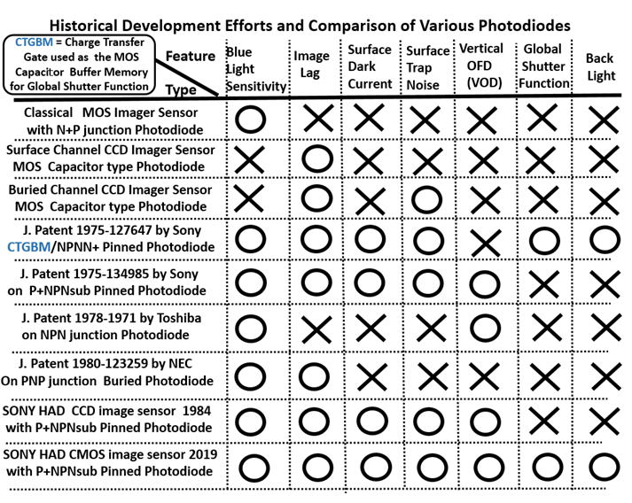
(1) N+P junction Photodiode deveoloped
with the simple DRAM MOS process.
with Serious Image Lag and Surface Large Dark Current,
without Global Shutter Function nor Vertical Overflow Drain
P.K.Wiener, et al
"A self-Scanned Solid State Image Sensor",
in Proc. IEEE,Vol 55, No.9, 1967.
G.P.Weckler,
"Operation of PN Junction Photo Detectors
in a Photon Flux Integrating Mode",
IEEE J. Solid State Circuits. Vol2, pp.65-73,
September 1967.
P.J.W. Noble,
"Self-Scanned Silicon Image Dector Arrys",
IEEE Trans. ElectronDevices, Vol.ED-15, No.4,
pp.202-209,1968.
S.G. Chamberlain,
"Photosensitivity and Scanning of Silicon Image
Detector Arrays" IEEE J.Solid State Circuits,
Vol.SC-4, No.6, pp.333-342, 1969.
F.L.J.Sangster and K.Teer, "Bucket Brigate
Electronics - New Possibilities for Delay
Time-Axis Conversion and Scanning",
IEEE J.Solid-State Circuits, VOL.SC-4, No.3,
pp.131-136, 1969.
W.M.Regitz and J.Karp,
"A Three-transistor-cell, 1024 bit, 500 nsec
MOS RAM", IEEE JSSC, VOl.SC-5, No.5,
pp.181-186, October 1970.
(2) Surface Channel CCD type
MOSCapacitor Photodioe
with Surface Trap Noise and Large Surface Drak Current
without Global Shutter Function nor Vertical Overflow Drain
W. S. Boyle and G. E. Smith,
“Charge-Coupled Semiconductor Devices,”
Bell Syst. Tech. J., 49, pp.587-593, 1970.
Amelio, G. F., M. F. Tompsett, and G. E. Smith,
“Experimental verification of the charge coupled
device concept,” Bell Syst. Tech. J. 49, 593. , 1970
Michael Francis Tompsett at Bell Lab,
“charge coupled devices,”
U.S. Patent No. 4085456, Aug 30, 1972 .
(3) Buried Channel CCD type
MOS Ccapacitor Photodioe
with Surface Trap Noise and Large Surface Drak Current
without Global Shutter Function nor Vertical Overflow Drain
R. H. Walden, R. H. Krambeck, R. J. Strain,
J. McKenna, N. L. Schryer, and G. E. Smith,
“The Buried Channel Charge Coupled Devices,”
Bell Syst. Tech. J., no.51, pp.1635-1640, 1972.
Boyle, W. S., and G. E. Smith, 1974,
“Buried channel charge coupled devices,”
U.S. Patent No. 3,792,322 February 12, 1974�.
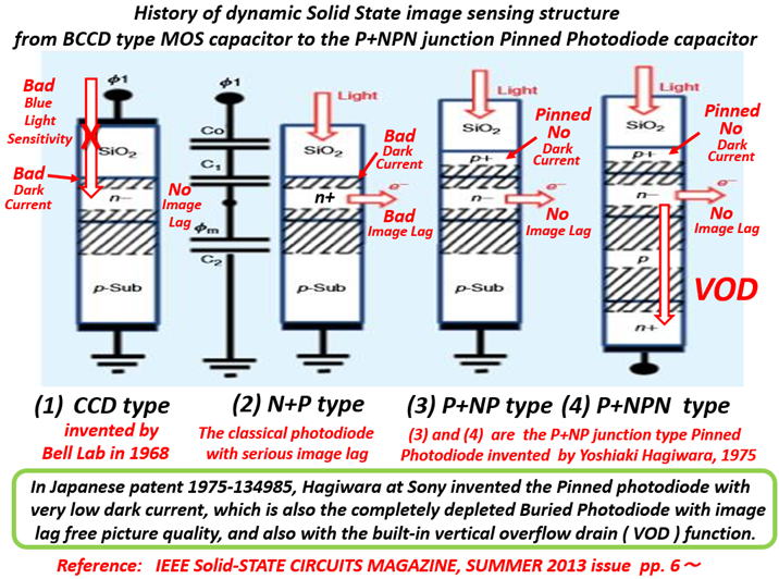
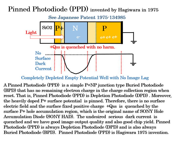
(4) P+NPNsub junction type Photodiode
invented by Hagiwara 1975
without Surface Trap Noise nor Large Surface Drak Current
with Vertical Overflow Drain (VOD) and Global Shutter Function.
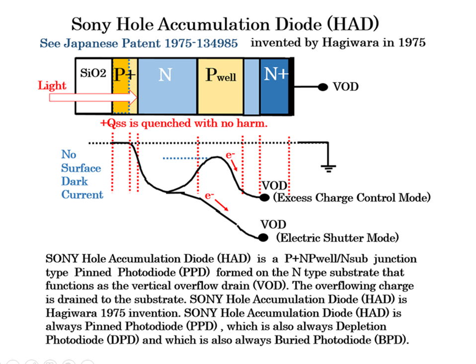
See Japanese Patent 1975-134985 for PDD with VOD Function
and also 1975-127647 for the PPD with Global Shutter Function.
Hagiwara at Sony filed on Oct 22, 1975
a Japanese Patents ( JP 1975-127647 )
on the NPN/Sub junction type Pinned Photodiode ,
with a built-in golobal shutter function using
a charge transfer gate also as the built-in global shutter
gate and also as a temporally MOS buffer capacitorance
next to the output charge tansfer device (CTD)
with the complete charge transfer operation mode
for very low image-lag action picture quality.
The other patent ( JP 1975-134985 ) is the invention of
the Pinned Photodiode with the built-in vertical overflow darin(VOD).
The surface is pinned. The surface is heavily doped and allowed
to have a metal ohmic contact. The heavily doped surface is a
heagily doped majority carrier hole accumulation region (SONY
original HAD senor ) and quenching the surface positively charge
fixed interface charge Qss and the trapping state Nss.
The signalelectron charge is solated from the silicon surface
interface and confined in the buried lightly doped N region for
the charge collection and storage.
So this 1975 Pinned Photodiode invention with no dark current
by Hagiwara in Sony is also the Buried Photodiode invention
with the complete charge transfer mode with no image lag feature.
See the details in the papers by Hagiwara Yoshiaki while
he was a PhD student at Caltech from 1972 to 1975.
"The Influence of Interface States on Incomplete Charge
TRansfer in Overlapping Gate Charge-Coupled Devices"
by Amr M.Mohsen, T.C.McGill, Yoshiaki Daimon Hagiwara,
and Carver A. Mead, IEEE Journal of Soild-State Circuits
Vol. SC.8 , No.2, April 1973
"Buried Channel CCD Charge Transfer" by Yoshiaki Hagiwara,
T.C.McGill, and Carver A. Mead, ISSCC1974 Paper
in Philadelphia, USA, February 1974
"Final Stage of the Charge-Transfer Process in Charge-Coupled
Devices" by Yoshiaki Daimon Hagiwara, Amr M. Mohsen, and
T.C.McGill, IEEE Transactions on Electron Devices, VOl. ED-21,
No.4, April 1974
(5) NPNsub junction type Photodiode Patent
with Vertical Oveflow Drain (VOD) function
by Yamada-san at Toshiba in 1978
This patent is overlapping with Hagiwara 1975-134985 patent
of the Pinned Photodiode with the built-in VOD function.
This patent is invalid. See Japanese Patent 1978-1971
The surface is not pinned. The surface is very unstable.
Yamada-san at Toshiba filed in 1978 a Japanese Patent
( JA 1978-1971 ) on Jan 13, 1978 on an NPNsub junction type
Vertical Overflow Drain (VOD1978) structure, which is
a derivative or duplicate patent of the Hagiwara 1975
invention ( JP 1975-134985 ) of the NPNsub junction type
Vertical Overflow Drain structure.
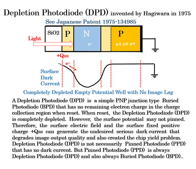
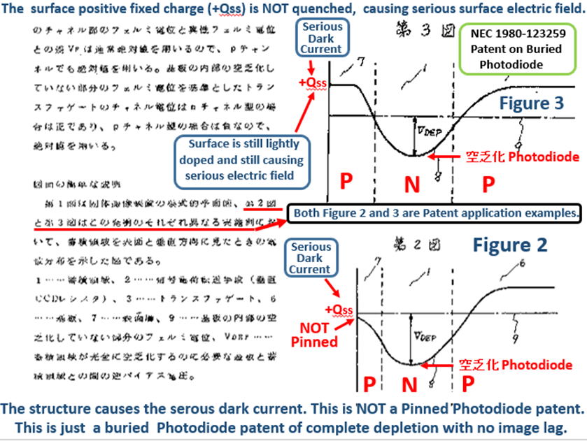
(6) PNPsub junction type Buried Photodiode Patent
by Shirai-san and Teranishi-san at NEC in 1980
This patent is overlapping with Hagiwara 1975 patent.
See Japanese Patent 1975-134985 for PDD with VOD Function
This patent is invalid. See Japanese Patent 1980-123259
This patent is about Buried Photodiode structure but
this is NOT a Pinned Photodeode structure, the surface
is not heavily doped and the strong electric field is
at the surface to create the serious dark current.
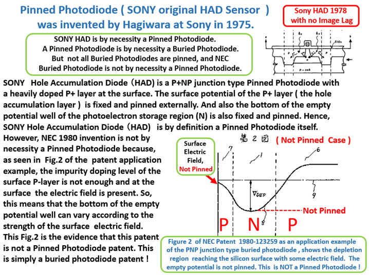
Teranishi-san at NEC did NOT invent the Pinned Photodiode !!!!
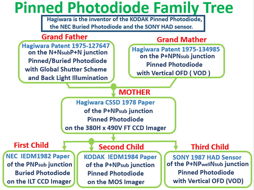
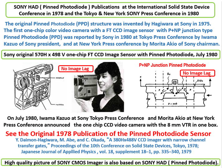
(7) The P+NP junction type Pinned Photodiode
developed by Hagiwara at Sony in 1978 and
used in the 380H x 490V FT CCD image sensor.
(8) The P+NP junction type Pinned Photodiode
developed by Hagiwara at Sony in 1979 and
used in one chip FT CCD image sensor.
(9) The N+PNsub junction type Photodioe
with the vertical overflow drain (VOD)
developped by Hitachi in 1980 and used
in one chip MOS image sensor.
(10)The PNP junction type Buried Photodiode
developed by Teranishi-san and his NEC team,
used in the ILT CCD image sensor and
published in IEDM1982.
Buried Photodiode in general does not have by necessity
the complete charge transfer mode which is needed for
the image lag free feature for fast camera action pictures.
.
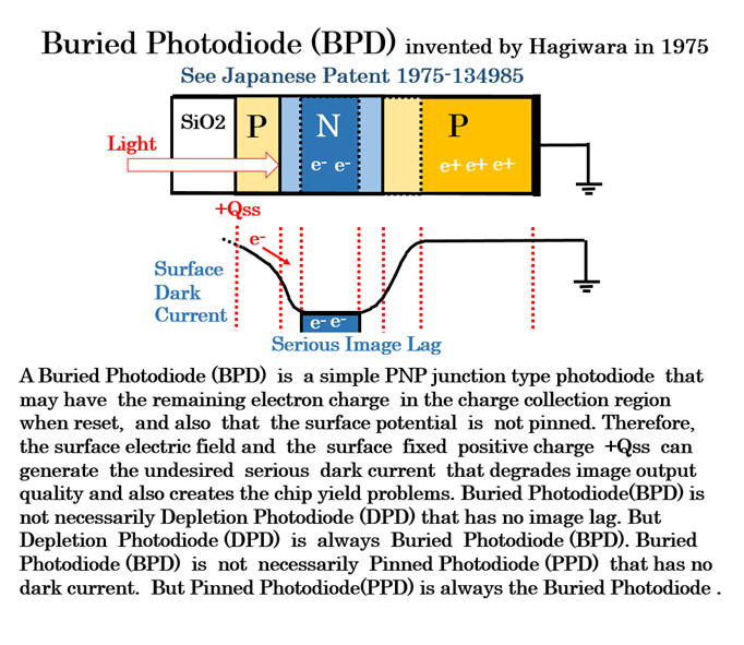
Buried Photodiode has to be operated in the complete charge
transfer mode which is called as the Depletion Photodiode that
has the image lag free feature for fast camera action pictures.
Y. Ishihara, E. Oda, H. Tanigawa, N. Teranishi,
E. Takeuchi, I. Akiyama, K. Arai, M. Nishimura,
and T. Kamata, “Interline CCD Image Sensor
with an Anti Blooming Structure,”
ISSCC Digest of Technical Papers,
pp.168-169, Feb. 1982.
N. Teranishi, A. Kohno, Y. Ishihara, E. Oda,
and K. Arai, “No Image Lag Photodiode
Structure in the Interline CCD Image Sensor,”
IEDM Tech. Dig., pp.324-327, 1982.
Y.Ishihara and K.Tanigaki,"
A High Photosensitivity IL-CCD Image Sensor
with Monolithic Resin Lens Array",
IEDM1983 Tech. Dig, pp.497-500,
December 1983.
B.C. Burkey et al, "The Pinned Photo Diode
for an Interline Transfer Image Sensor",
IEDM1984, Dig.Tech.Papers, pp.28-31, Dec1984.
They all did not know that Hagiwara invented this
Pinned Photodiode in 1975 and filed in Japanese
Patents (1975-127647 and 1975-134985).
(11) The P+NPNsub junction type Pinned Photodiode
with the VOD function invented by Hagiwara in 1975,
developed in 1984 by the SONY team, and named
as SONY original HAD sensor.
SONY HAD ( Pinned Photodiode ) was perfected
by the following two works by Sony Engineers.
K. Ishikawa and T. Iizuka,
"One inch 2M pixel CCD with Hyper HAD sensor
and Camera System for HDTV", SPIE proc.
Vol. 1656, pp.30-40, February 1992.
K. Yonemoto and H. Sumi ,
"A CMOS Image Sensor with a Simple FPN Reduction
Technology and a Hole Accumulation Diode",
ISSCC2000, Dig.Tech.Papers, pp.102-103, February 2000.
**********************
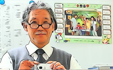
The AIPS image sensor watching at its inventor, Yoshiaki Hagiwara.
return to the TOP Page
**********************