**********************
The AIPS ( Artificial Intelligent Partner System ) Home Page 019
**********************
*******************************************************************
Questions by Prof. Albert Theuwissen are ,
- who invented and developed the stitching technology
for large area image sensors ?
- who owns the world record in low-noise
in the voltage domain for CMOS Image Sensor (CIS) ?
Hagiwara believes that
Hagiwara invented and Sony diligent engineers developed the stitching technology
for large area image sensors. SONY called SONY original HAD sensor.
But the technical world ignored the SONY businesss Brand Name HAD, and
called it by another name, the Pinned Photo Diode.
Sony diligent engineers developed and now Sony owns the world record in
low-noise
in the voltage domain for CMOS Image Sensor (CIS).
Teranishi did not invent the Pinned Photo Diode.
Hagiwara is the inventor of the Pinned Photo Diode.
Fossum is not the inventor of the active image sensor picture element.
Peter Noble is the inventor of the active image sensor picture element.
http://www.pjwn.co.uk/
******************************
***********************************************************************
**********************
これは70歳じじいのぶつぶつぼやきの独り言でした。
**********************
**********************
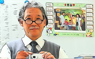
The AIPS image sensor watching at its inventor, Yoshiaki Hagiwara.
return to TOP Page
**********************