**********************
The AIPS ( Artificial Intelligent Partner System ) Home Page 011
**********************
*******************************************************************
萩原の母校のCaltech での在学時代、萩原は教授から
The truth shall you make you free.
という言葉を良く授業で聴かされました。その意味が、
萩原は、この歳、70歳になり、しみじみと感じています。
*******************************************************************
これは発明協会の公式WEBサイトからの引用内容です。萩原はその記述内容に反論しています。
http://koueki.jiii.or.jp/innovation100/innovation_detail.php?eid=00059&test=open&age=
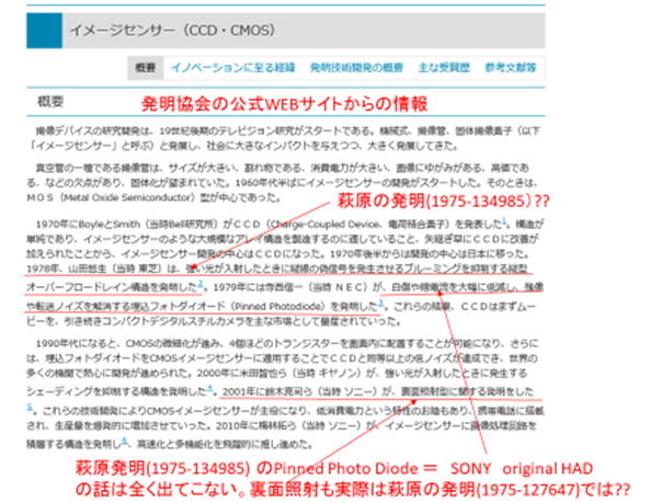
この掲示には、SONYが誇る SONY original HAD のことは一言も引用がありません。
実は SONY original HAD は SONYの萩原の発明であり、多くのSONYの勤勉な技術者の
努力により完成した技術です。その努力と成果が全く無視されていることは非常に残念です。
以下にその根拠を説明するために萩原の1975年の2つの特許の説明をします。
*******************************************************************
Cool Facts of Image Sensor History
*******************************************************************
Cool Fact (1)
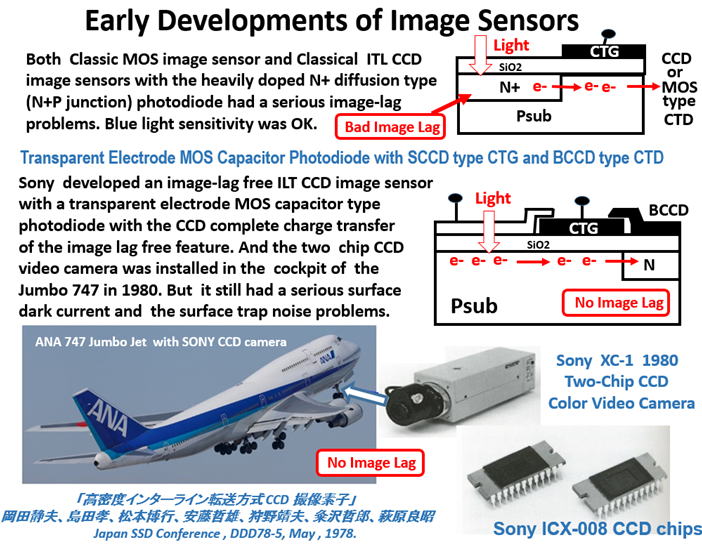
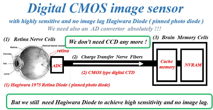
SONY announced in 1978 the one chip image-lag-free FT CCD image sensor
with the Pinned Photo Diode, Hagiwara 1975 invention. Hagiwara himself
designed
the chip, developed the Pinned Photo Diode process fabrication flow sequence
and the CCD camera control system, all of them by Hagiwara himself alone
in 1976.
Many doubted the success, but after the prototype was made in 1977 by Hagiwara
alone, many joined Hagiwara work and helped Hagiwara.

Cool Fact (2)
The Pinned Photo Diod, Hagiwara 1975 invention whichis, in Sony, called
as
the SONY original HAD sensor, is still used in the modern digital CMOS
image
sensor with the back light illumination scheme which was proposed in 1975
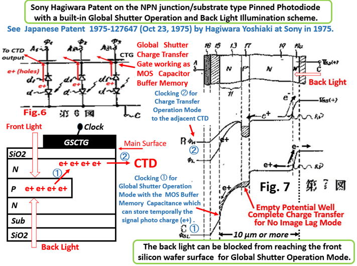
by Hagiwara of SONY in Hagiwara Japanese Patent ( 1975-127647 ).
The Back Light Illumination type Pinned Photo Diode Sensor
invented by Haiwara of SONY. See Japanese Patent ( 1975-127647).
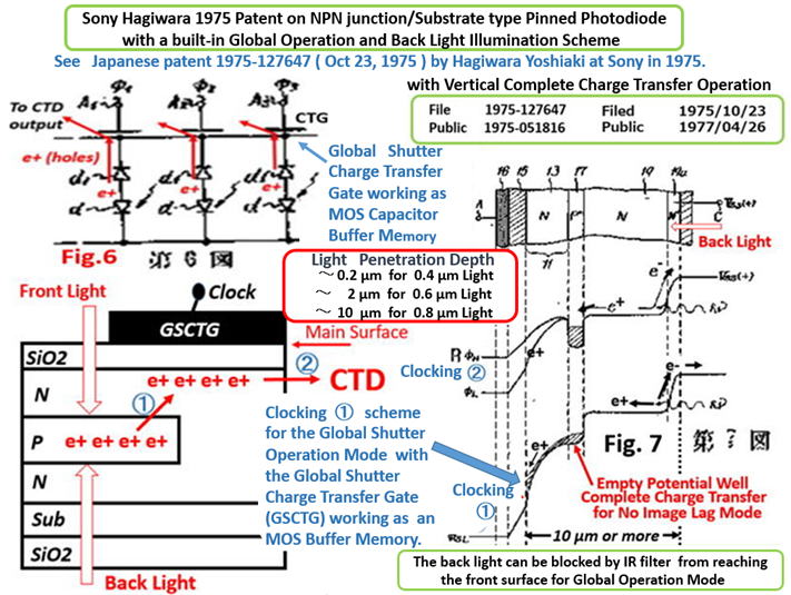
The Back Light Illumination type Pinned Photo Diode Sensor
invented by Haiwara of SONY. See Japanese Patent ( 1975-127647).
Cool Fact (3)
SONY announced in 1980 the two-chip image-lag-free IL CCD image sensor
with the picture cell structure of the transparent electrode with the lateral
overflow drain. The two chip type image-lag-free IL CCD video camera was
sold to ANA and was installed in the cock pit of the 747 jumbo jet. Hagiwara
designed and developed the two-chip image-lag-free IL CCD image sensor.
Cool Fact (4)
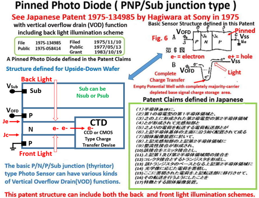
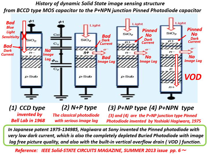
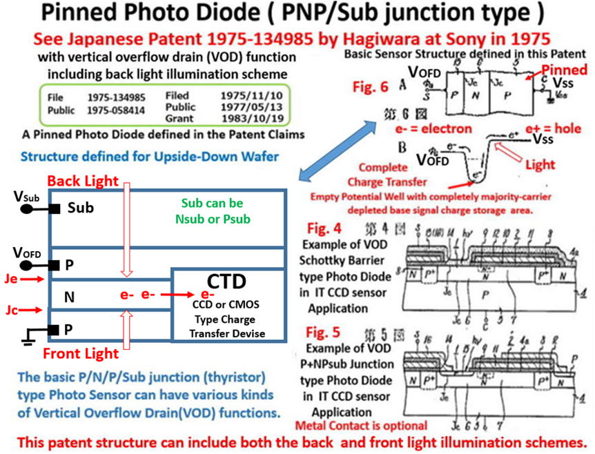
SONY won the SONY vs Fairchild Patent War ( 1991-2000 ) on the P+NPNsub
junction ( thyrisor ) type Pinned Photo Diode with the Vertical Overflow Drain
Function invented by Hagiwar ( JAP 1975-134985 ).

Cool Fact (5)
SONY won the Secret Patnet War against NEC Teranish Patent on the Hagiwara 1975
P+NPNsub junction ( thyrisor ) type , completely image-lag-free Pinned
Photo Diode
Patent ( JAP 1975-134985) against the NEC 1979 Teranishi Patent on the
Buried
Photo Diode which was published in IEDM1982.

Hagiwara did not understand why Fossum was insulting Hagiwara
and SONY pride and honor. Fossum is a fake commentator. And
Fossum 2014 paper is a fake paper with WRONG conclusions.
Hagiwara and SONY engineers are not happy at Fossum and Teranish.
Cool Fact (6)
(Question)- who invented and developed the stitching technology
for large area image sensors ?
Hagiwara invented and Sony developed the stitching technology
for large area image sensors and named the technology as the
SONY original Hole Accumulation Diode (HAD) sensor.
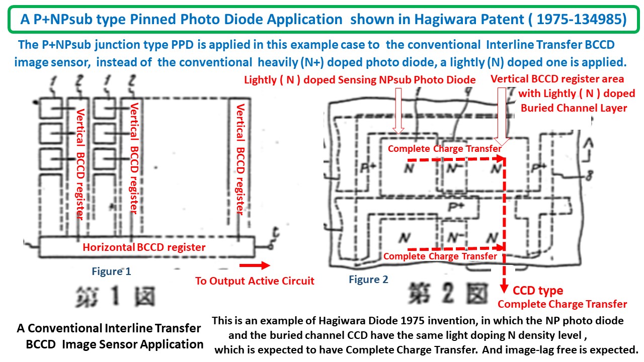
Hagiwara invented it , in the Japanese 1975 patent ( 1975-134985 )
as the P+NPNsub junction ( Thyristor ) type Light Detecting Picture
Cell Structure which is now known widely as the Pinned Photo Diode.
As one of the Hagiwara 1975 patent application for large area image
sensors, Hagiwara drew in the Patent Figure the large scale Interline
Transfer CCD Image sensor as a possible application.
Sony deligent engineers, including Hagiwara, developed, the stitching
technology for large area image sensors. SONY called the technology
in SONY business as the SONY original HAD sensor . Naturally, the
technical world did not use the SONY business Brand Name HAD,
and called it by another name, the Pinned Photo Diode. But the
Pinned Photo Diode and SONY original HAD technology are the
same thing, both invented by Hagiwara in 1975.
Teranishi did not invent the Pinned Photo Diode.
Hagiwara is the inventor of the Pinned Photo Diode.
Cool Fact (7)
(Question) - who owns the world record in low-noise
in the voltage domain for CMOS Image Sensor (CIS) ?
Sony deligent engineers developed and now Sony owns
the world record in low-noise in the voltage domain for CMOS
Image Sensor (CIS) with the Pinned Photo Diode with the
Back Light Illumination, that was also invented by Hagiwara of
SONY in 1975 the Japanese 1975 patent ( 1975-127647 ).
Fossum did not develop the modern digital CMOS image sensor
The Sony deligent engineers developed the modern digital CMOS
image sensor.
Fossum is not the inventor of the active image sensor picture
element. Peter Noble is the inventor of the active image sensor
picture element. See http://www.pjwn.co.uk/
Cool Fact (8)
(Question) - Who won on the SONY-Kodak Patent War on Digital Camera ?
SONY and Kodak made an agreed in 2007 to use each other's patents on
the Small and Handy Digital Camera Technology.
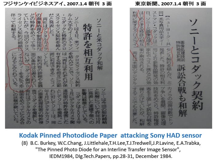
Digital Camera by definition must be small and handy as originally conceived
by SONY with many semiconductor components, including the image sensor,
ADC, Fast Cache SRAM, the slow Nonvolatile memory chip and other digital
image processing units. One single engineer cannot develop all of it alone.
Many SONY deligent enginneers worked hard and developed the modern
CCD and CMOS digital Camera, with the P+NPNsub junction (thyristor)
type Light Dectecting Photo Diode ( JAP 1975-134985 ) and the N+NPN
junction type Buried Photo Diode ( JAP 1975-127647 ) with the back
light illumination scheme, both invented in 1975 by Hagiwara of Sony.
One person can invent it, but the many years of the hard working efforts
of many deligent people are needed to realize it.
*******************************************************************
萩原の母校のCaltech での在学時代、萩原は教授から
The truth shall you make you free.
という言葉を良く授業で聴かされました。その意味が、
萩原は、この歳、70歳になり、しみじみと感じています。
*******************************************************************
**********************
これは70歳じじいのぶつぶつぼやきの独り言でした。
**********************
**********************
The AIPS image sensor watching at its inventor, Yoshiaki Hagiwara.
return to TOP Page
**********************