**********************
The AIPS ( Artificial Intelligent Partner System ) Home Page 002
hagiwara-yoshiaki@aiplab.com
Return to http://www.aiplab.com/
**********************
For full English versions, please visit the following sites.
Story of Pinned Photo Diode (html)
Hagiwara at SONY is the true inventor of Pinned Photo Diode (html)
See also ElectronicsStackExchangeSite on "What is Pinned Photo Diode ? "
Pinned Photo Diode was invented by Hagiwara of Sony in 1975 (PDF)
**********************
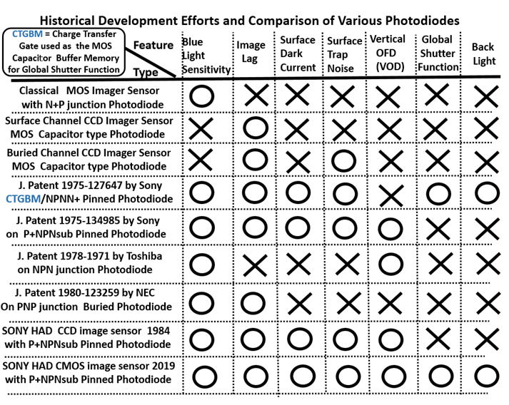
What is Pinned Photo Diode ?
Pinned Photo Diode is a light detecting photo diode structure
of a P+NP junction type in the substrate die which can be
applied to all kinds of the charge transfer device (CTD),
including CCD and CMOS image sensors. The signal electrical
charge is stored in the center N region. The surrounding top
P+ region is fixed or pinned to an externally controllable stable
voltage value. Both P+ and P region can be electrically connected
in common applications. Pinned Photo Diode is a dynamically
operating PNP junction. The center (buried) N region is floating
and dynamically operated. The top P+ region protects the base
N region from the top SiO2 surface trap interface states. Hence,
Pinned Photo Diode is free from the surface trap noise. Since
there is no SiO2 surface electric field, Pinned Photo Diode is
free from the surface electric field generated dark current.
The signal electrical charge is to be transferred to the adjacent
charge transfer device (CTD) thru the charge transfer gate with
complete charge transfer mode. This gives the feature of the
image lag free picture quality and more advantages as shown below.
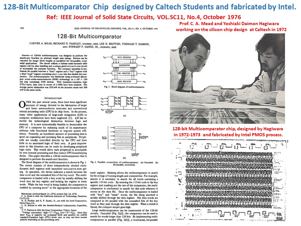
Who invented Pinned Photo Diode ?
The pinned photo diode was originally invented and defined
by Hagiwara of Sony in the three 1975 Hagiwara patents
( JAP 1975-127646, JAP 1975-127647 and JAP 1975-134985 ).
In these three Hagiwara 1975 patents, it was explained that
the light detecting structures defined in the patent claims
have many degrees of freedom in operational modes and also
can be applied , not only to the conventional frame transfer
and interline transfer CCD imagers but also to other charge
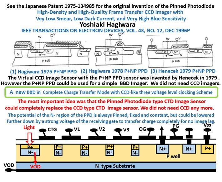
transfer devices, that include BBD and CMOS image sensor.
The completely image lag free Interline Transfer CCD image sensor
with the Pinned Photo Diode light detecting structure was invented
by Hagiwara in his 1975 patent applications. Teranish did not invent
the Pinned Photo Diode. Teranishi was one of the many developpers
of the Pinned Photo Diode, that include the diligent and hard working
Sony image sensor engineers including Hagiwara. Moreover, Teranish
did not invent the image lag free Interline Transfer CCD image sensor.
Teranishi was one of the many developpers of the completely image
lag free Interline Transfer CCD image sensor, that include the silent
and honest Sony image sensor engineers including Hagiwara. Hagiwara
invented the Pinned Photo Diode in 1975. Hagiwara invented also the
completely image lag free Interline Transfer CCD image sensor in 1975.
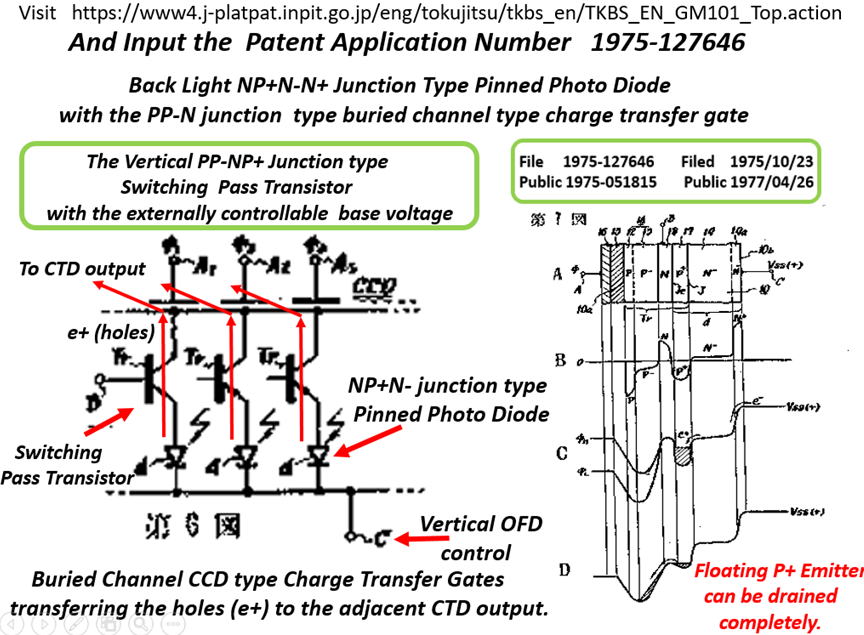
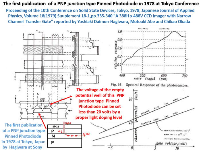
The first one is the Hagiwara JAP 1975-127646 in which the
PP-NP+NN+ junction type Pinned Photo Diode with Back Light
Illumination Scheme was defined with the PP-N type buried
channel charge transfer gate. The PP- layer is the buried channel.
Addition to that, the PP-NP+ junction functions as a switching
pass transistor with the P+ emitter as the floating charge storage
area while the base N region voltage is externally controlled.
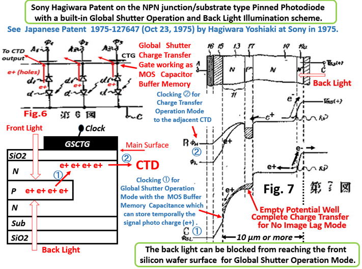
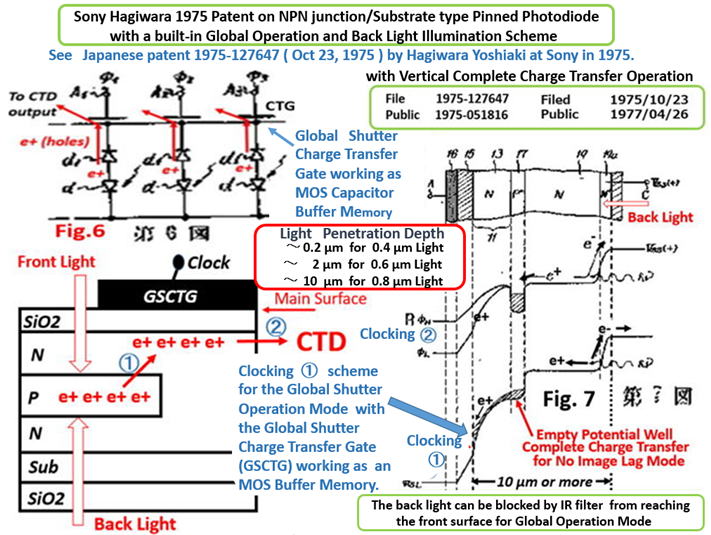
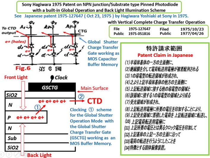
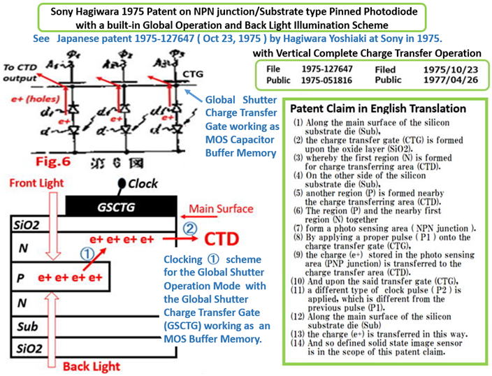
The second one is the Hagiwara JAP 1975-127647 that defines
the N+NPN junction type Buried Photo Diode structure with
the surface channel type charge transfer gate with Back Light
Illumination. The signal charge stored in the P region can be
transferred completely.
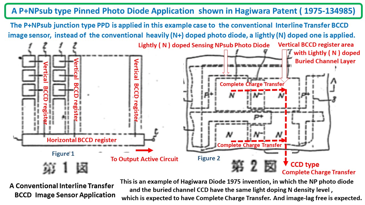
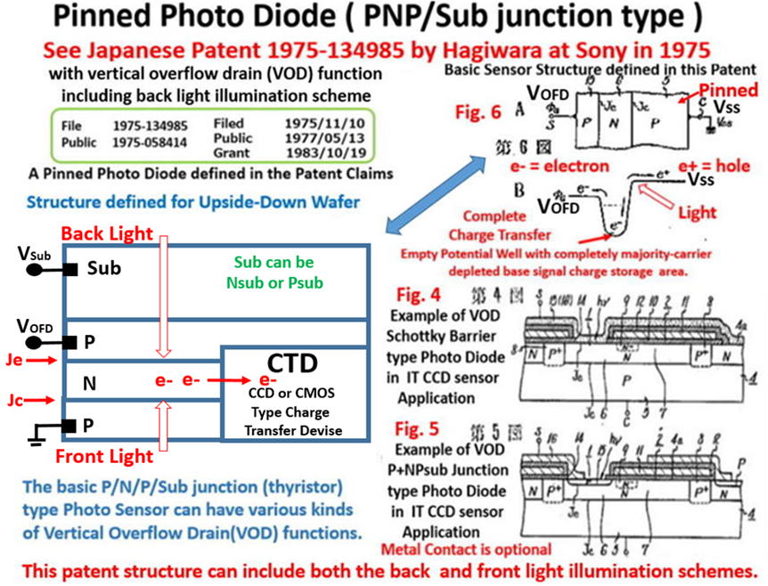
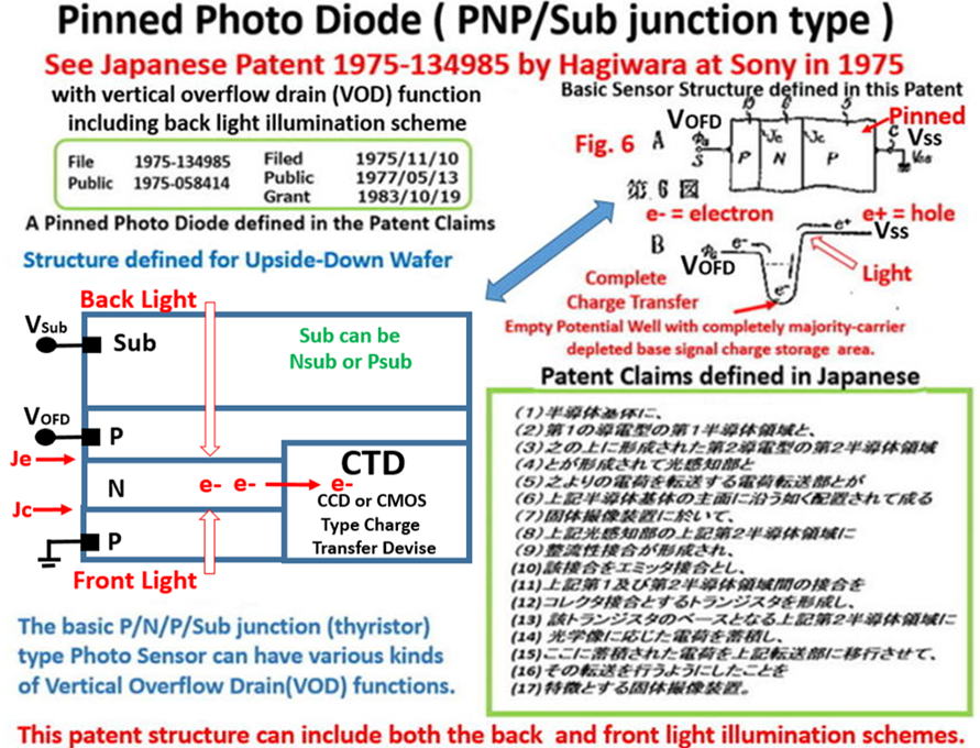
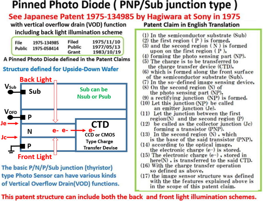
The third one is the Hagiwara JAP 1975-134985 in which the
P+NPNsub junction (thyristor) type Pinned Photo Diode was
defined in the Patent Claim Scope with the charge transfer
gate of the buried channel type as an example in the ITL type
CCD image sensor type patent application example. In the patent
application examples, it is shown that the PNP jnction transistor
type structure has more degrees of freedom and can have
inherently the built-in vertical overflow drain (VOD) function.
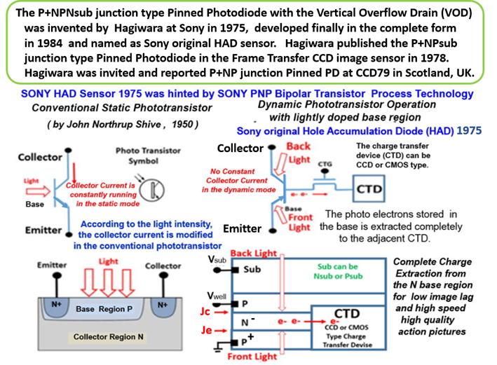
Sony original Hole Accumulation Diode (HAD) and Pinned
Photo Diode (PPD) are the same thing. Both were invented
by Hagiwara in 1975. An example was given for a large area
ITL type CCD image sensor type patent application. But
applications are not limited to the ITL type CCD image sensor.
The patents can be applied to all kinds of charge transfer devices.

************************************************
to next Page003
Return to http://www.aiplab.com/
******************************************************************