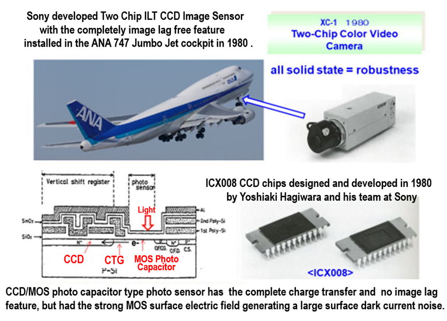
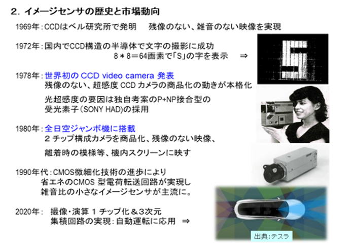
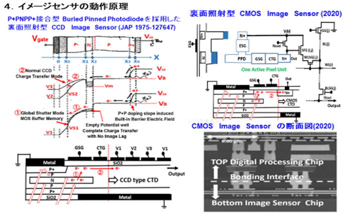
Hagiwara at Sony invented Pinned Photodiode in 1975
***********************************************
Pinned Photodiode was invented by Hagiwara in 1975
***********************************************
For Japanese language, visit http://www.ssis.or.jp/
For English language, visit http://www.ssis.or.jp/en/index.html
************************************
Semiconductor History Museum of Japan
************************************
For Japanese language, visit https://www.shmj.or.jp/
For English language, visit https://www.shmj.or.jp/english/index.html
*******************************************************************
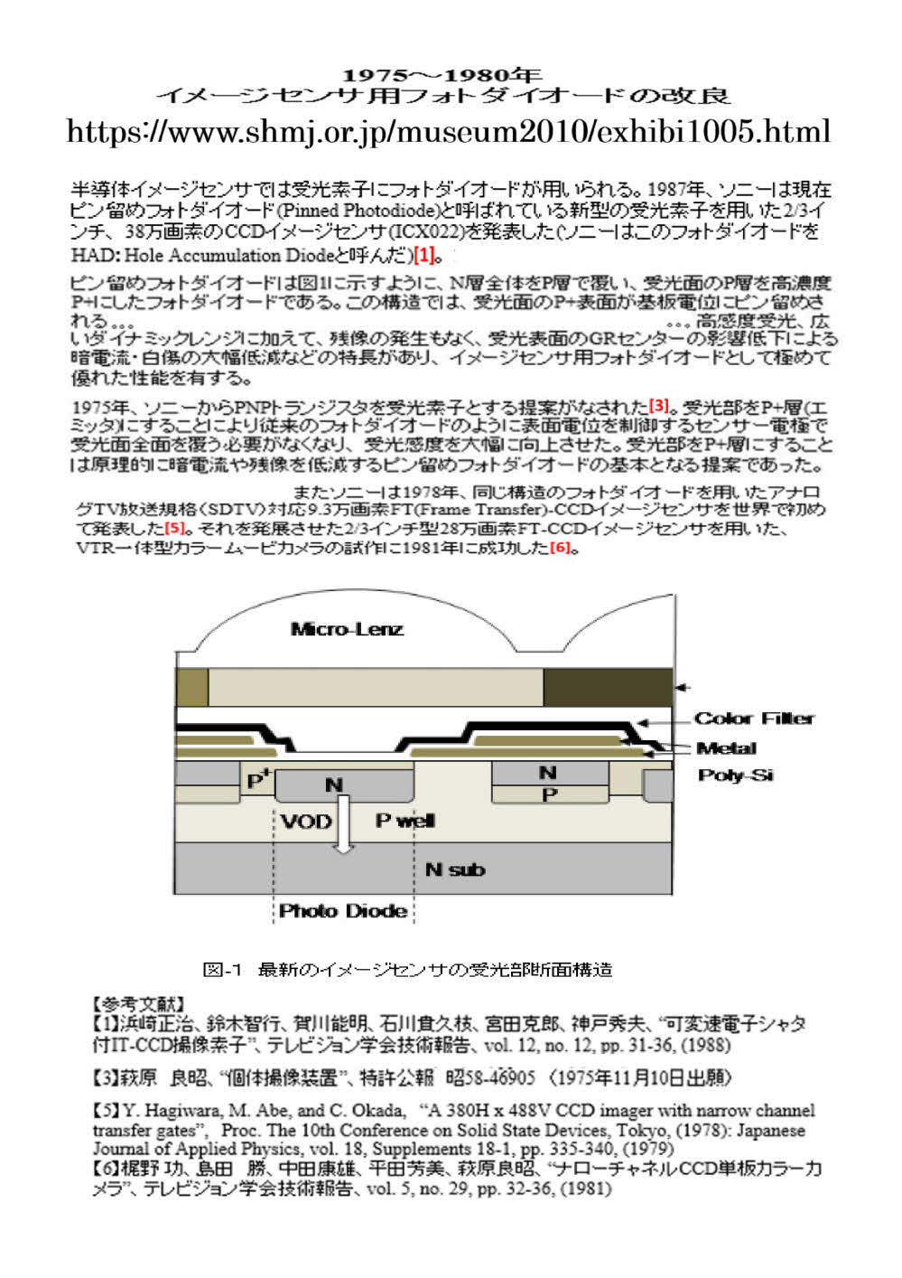
Review of Early Developments of Image Sensors in Japan
*******************************************************************
https://www.shmj.or.jp/museum2010/exhibi1005.html
******************************************************************
***********************************************************
Review of Early Developments of Image Sensors in Japan
***********************************************************
Semiconductor History Museum of Japan says
Yoshiaki Hagiwara at Sony invented the Pinned Photodiode in 1975
***********************************************************
https://www.shmj.or.jp/english/pdf/dis/exhibi1005E.pdf
*******************************************************************
*******************************************************************
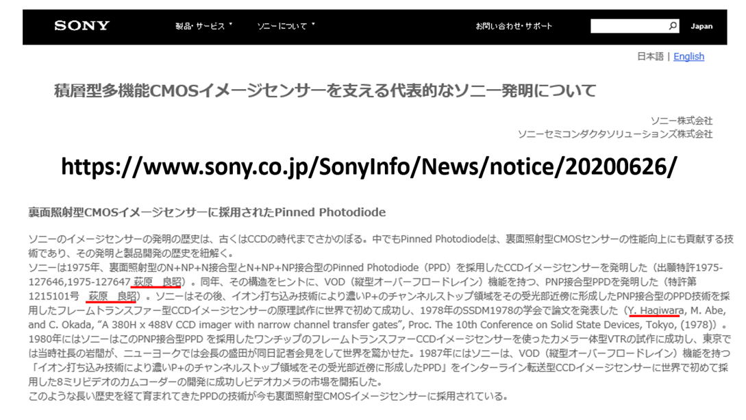
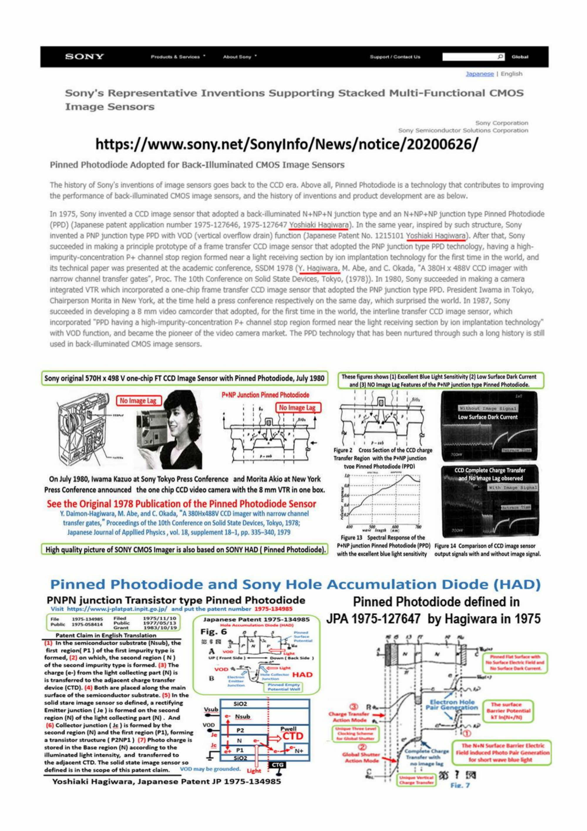
SONY explained that Hagiwara at Sony invented Pinned Photodiode in 1975.
*******************************************************************
https://www.sony.net/SonyInfo/News/notice/20200626/
*******************************************************************
SONY explained that Hagiwara at Sony invented Pinned Photodiode in 1975.
*******************************************************************
https://www.sony.co.jp/SonyInfo/News/notice/20200626/

*******************************************************************
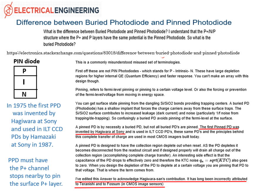
The WEB site also explained that Hagiwara invented Pinned Photodiode in
1975.
*******************************************************************
**********************
埋込込みPhotodiodeと Pinned Photodiodeの相違点
**********************
●匿名の人からの投稿ですが、埋込みPhotodiodeと Pinned Photodiodeの相違点を的確に説明しています。
そして NECの寺西さんは 埋込みPhotodiodeの受光素子を世界ではじめて ILT CCD に採用しましたが
その IEDM1982の論文には 実際には 残像が存在します。その論文で報告した受光素子は従って正確には
Pinned Photodiodeでなかった事を自らが論文で中での実測dataで明示した論文であると解釈されます。
「もとNECの寺西さんを間違ってPinned Photodiodeの発明者として過大評価した」と明記しています。
https://electronics.stackexchange.com/questions/83018/difference-between-buried-photodiode-and-pinned-photodiode
************************************************************
Hagiwara at Sony invented Pinned Photodiode in 1975
index000_Invention_of_Pinned_Photodiode_in_1975.html
index001_Image_Sensor_1975_1977_and_2014_Patents.html
index002_Facts_on_Invention_of_Pinned_Photodiode.html
index003_Hagiwara_Publication_List.html
index004_My_Wonderful_Memory_Pictures.html
index005_Image_Sensor_Story_by_Hagiwara.html
index006_Slide_Sony_Atsugi_Tech_2020_07_10.html
*************************************************************
*********************************************************************
http://www.aiplab.com/index_Page001_E_Tegami.html
http://www.aiplab.com/index_Page002_Waka.html
http://www.aiplab.com/index_Page003_Enoy_Hungle.html
*********************************************************************
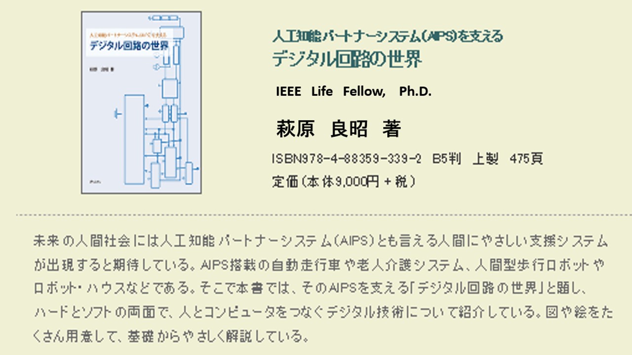
Yoshiaki Hagiwara wrote a book on
"the World of Artificial Intelligent Digital Circuits",
which is important and needed to built
the intelligent image sensor systems.
ISBM978-4-88359-339-2
Hard Cover, 460 page,
\ 9000 Japanese Yen + tax
If you are interestied in the book, Please visit
https://www.seizansha.co.jp/ISBN/ISBN978-4-88359-339-2.html
https://www.seizasha.co.jp/
********************************************************
hagiwara-yoshiaki@aiplab.com http://www.aiplab.com/
hagiwara@ssis.or.jp http://www.ssis.or.jp/en/index.html
********************************************************
******************************
Return to Top Page
http://www.aiplab.com/
*********************************