**********************
AIPS ( Artificial Intelligent Partner System ) Homepage 007
hagiwara-yoshiaki@aiplab.com
**********************
**********************
これは70歳じじいのぶつぶつぼやきの独り言です。
(7) Pinned Photodiode 特許戦争
**********************
SONY がどうして世界で image sensor business で世界をリード
し制覇しているのでしょうか?
SONYのHADセンサーは、1975年SONYの萩原の発明ですが、
その特性がほかの種類のセンサーと比較して、抜群の特性を持つ
ことが、この表から読み取れます。
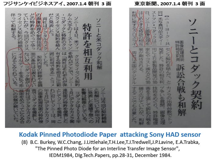
SONYはそのHADセンサーの特許を所有し、多くのライバル企業
からの知的財産問題提起や特許戦争で勝利し、時には和解して
共存の道を選び、イメージセンサーのビジネスを守ってきました。
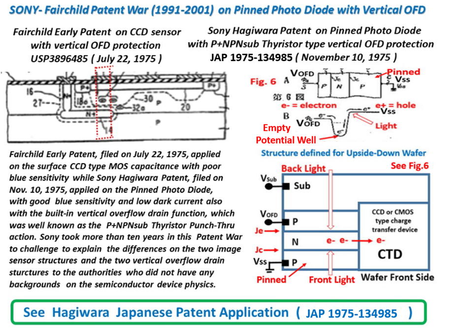
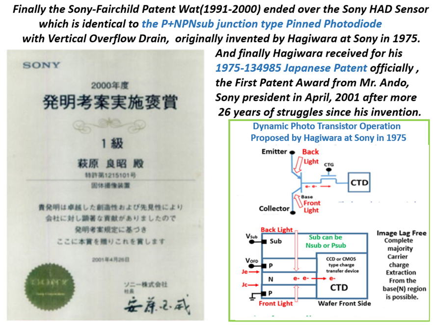
Hagiwara helped SONY for many years in the SONY-Fairchild,
SONY-Kodak, SONY-CalTech and SONY-NEC Patent Wars.
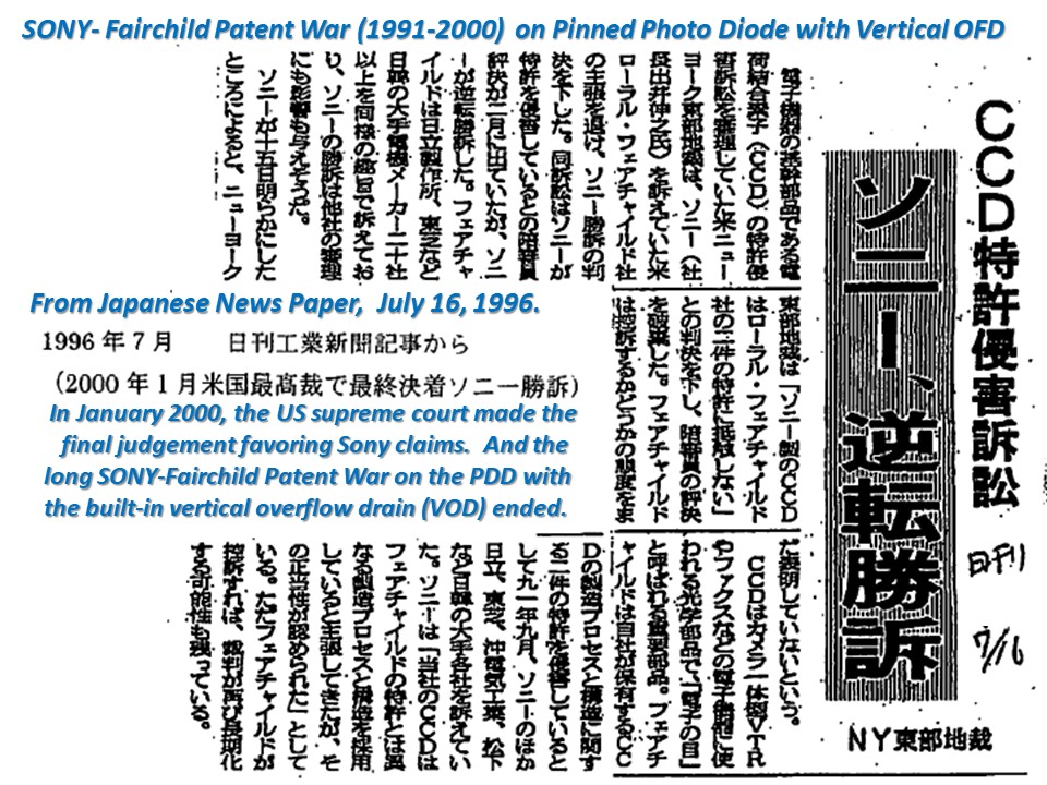
Among them, the SONY-Fairchild Patent War (1991-2000) was
the longest and worst Cold War not only for SONY but also for
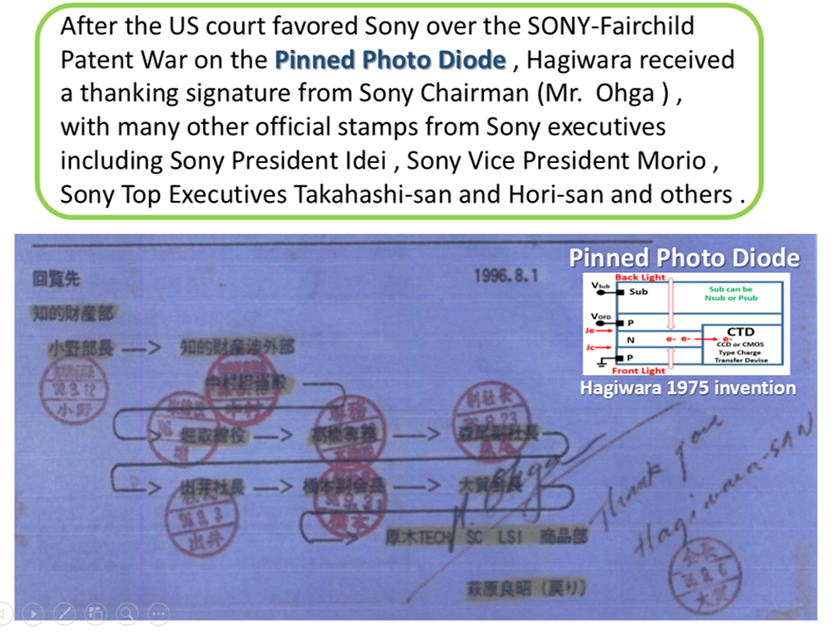
Hagiwara, the inventor of SONY HAD sensor. But finally SONY
won the SONY-Fairchild Patent War and Hagiwara became the
hero in Sony, recieving many thankful notes from SONY TOP.
SONY and Hagiwara both were very tired with the worst and
longest Fairchild-SONY Cold Patent War. And Sony made
friendly mutual technical agreements with JPL/CalTech and
KODAK patent issues on the SONY HAD sensor patents while
NEC was very persistant on their claim favoring the NEC 1980
Buried Photodiode patent against the Hagiwara 1975 patent of
the SONY HAD sensor. The result was clear. NEC gave up
image sensor business.
Hagiwara was finally awarded officailly in SONY
as the inventor of the SONY HAD sensor.
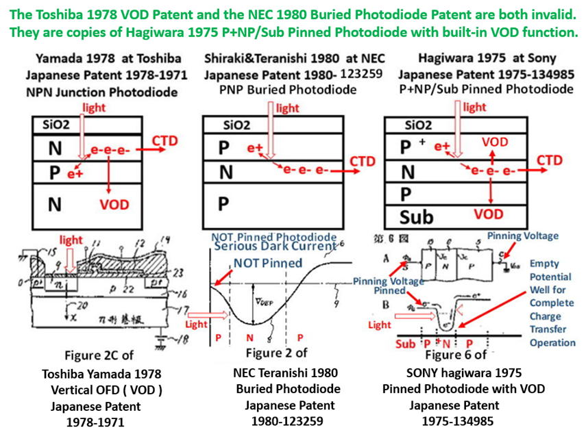
また、 NECとSONYとの特許戦争では、
実際にSONYのHADとNECの埋め込みPhotodiodeとの
水面下の特許戦争にかかわる文書が残っています。
NEC1980年特許とSONY1975年萩原特許との間の特許戦争
NECは負けてSONYが勝ち、その結果、敵対していたNECは特許
戦争に負けてビジネスが傾く、image sesnor のビジネスから撤退
したという醜い冷酷なお金の亡者の特許戦争が裏にありました。
NEC Buried Photodiode was not Pinned Photodiode (SONY HAD)
and finally NEC had to give up image sensor business and left
silently as the loser of the cold SONY-NEC patent war.
The Teranishi 1980 Buried Photodiode Patent was only focused
on the completely depleted photodiode feature that provides the
image lag free picture quality. However the NEC Teranish patent
actually did not have the important feature of the P+ layer of
hole accumulation (SONY HAD sensor feature ) to have the pinned
surface potential which is needed to quench the surface electric
field causing the serious dark current and low chip yield problems.
NEC could not produce the image sensor chips with reasonable
yeild since they did not know the knowledge of the positively
charged surface interface states Qss problems and did not know
how to quench the surface electric field problems causing the
serious surface dark current and yeild problems. NEC had to
give up image sensor business and left silently also as the loser
of the cold SONY-NEC patent war.
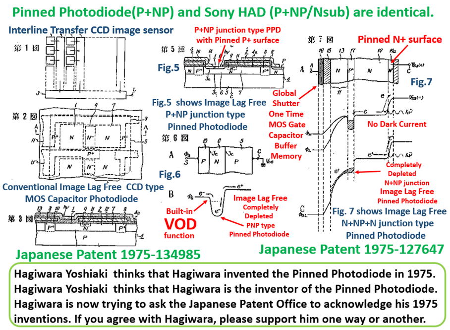
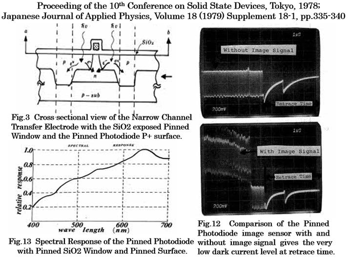
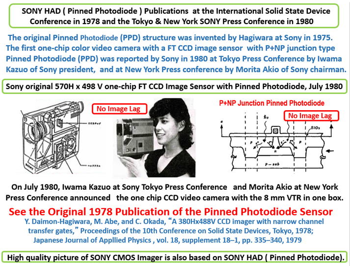
The First publication of Pinned Photodide by Hagiwara 1975.
P+NP_junction_type_Pinned_Photodiode_1978_Paper_by_Hagiwara (PDF)
*************************
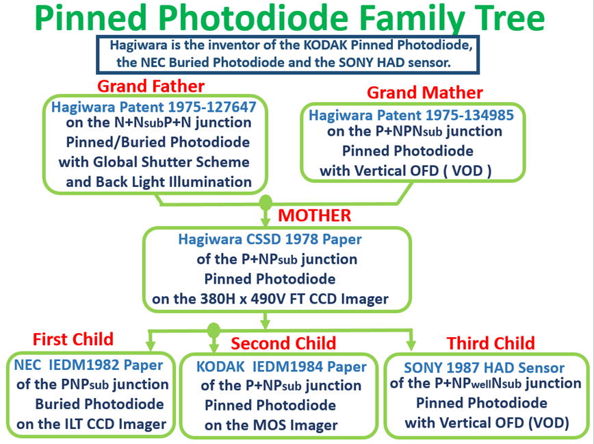
Hagiwara is the inventor of the KODAK Pinned Photodiode,
the NEC buried Photodiode and the SONY HAD sensor.
SONY がどうして世界で image sensor business で世界をリード
し制覇しているのでしょうか?
SONYのHADセンサーは、1975年SONYの萩原の発明ですが、
その特性がほかの種類のセンサーと比較して、抜群の特性を持つ
ことが、この表から読み取れます。
SONYはそのHADセンサーの特許を所有し、多くのライバル企業
からの知的財産問題提起や特許戦争で勝利し、時には和解して
共存の道を選び、イメージセンサーのビジネスを守ってきた結果です。
**********************
The AIPS image sensor watching at its inventor, Yoshiaki Hagiwara.
return to the TOP Page
**********************