**********************
AIPS ( Artificial Intelligent Partner System ) Homepage 0006
hagiwara-yoshiaki@aiplab.com
**********************
**********************
これは70歳じじいのぶつぶつぼやきの独り言です。
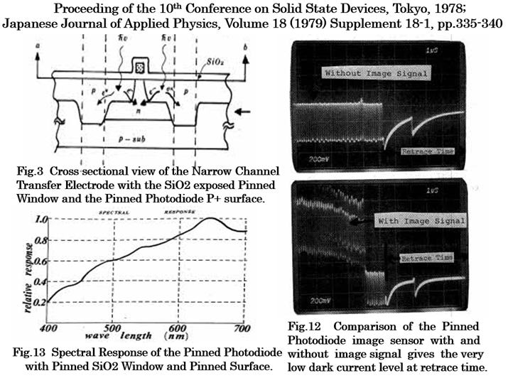
(6) 萩原の1978年のPinned Photodiodeの論文
**********************
P+NP_junction_type_Pinned_Photodiode_1978_Paper_by_Hagiwara (PDF)
*******************************
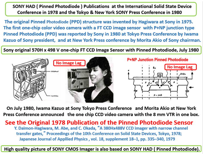
SONY developed this One chip FT CCD image sensor with
the simple lateral overflow drain structure of a simple
fabrication process designed for mass imager production..
Hitachi had already developed the One Chip MOS image
sensor with the virtucal oveflow drain (VOD) structure.
SONY was very cautious to apply the VOD structure
for SONY CCD image sensor fabrication process for
mass imager production in mind.
Many problems were to be solved before to apply the
VOD structure for the Interline transfer CCD imager.
SONY developed the P+NPNsub junction type Pinned
Photodiode sensor with the vertical overflow drain (VOD)
in 1984. SONY called the product as the SONY original
Hole Accumulation Diode (HAD) which is Hagiwara 1975
invention. See Japanese Patent 1975-134985. It took
for SONY another three years of time and efforts to
obtain the mass production technology and skill. And
in 1987 Sony finally introduced SONY HAD CCD imagers
in the Video Camera Markets around the world.
SONY HAD, Hagiwara 1975 invention, became strong.
Hagiwara 1975 invention is the origin of the SONY HAD, which has
another name of Pinned Photodiode.
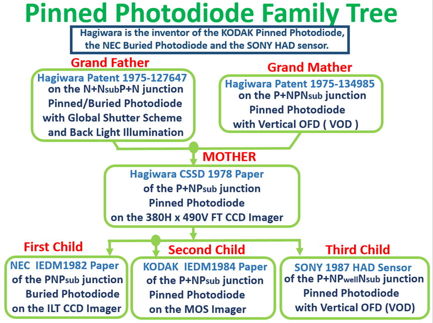
All the modern electronics eyes belong to the Family Tree of
SONY HAD, or the Pinned Photodiode Family Tree.
萩原の1975年の発明は、現在のすべての「電子の目」の
Pinned Photodiode Family Tree の源となる発明です。
**********************
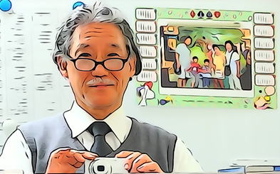
The AIPS image sensor watching at its inventor, Yoshiaki Hagiwara.
return to the TOP Page
**********************